What are the differences between SONET/SDH and OTN?

This blog posts highlights differences between OTN and SONET/SDH. It also provides links to other blog posts that focus on these differences in detail.

SONET/SDH and OTN are standard protocols for transporting signals from Point A to Point B on (mostly) optical fiber. 

However, there are some key differences:

  1. OTN (at least for OTU1 through OTU4) has a fixed frame size.  SONET/SDH does not.
  2. SONET/SDH has a fixed frame repetition rate (8000 frames/sec).  OTN does not.
  3. When mapping/muxing lower-speed tributary signals into higher-speed signals, SONET/SDH requires that all the lower-speed tributary signals be synchronous with each other and with the high-speed server signal.  OTN does not need this. 
  4. OTN has a standard FEC (Forward Error Correction) mechanism.  SONET/SDH does not have such a thing. 
  5. OTN offers more extensive TCM (Tandem Connection Monitoring) support than does SONET/SDH.
  6. The SONET/SDH standards only support data rates of up to 40Gbps (or OC-768).  The OTN standards support over 100Gbps (e.g., 200Gbps, 400Gbps, etc.)
  7. The mechanisms for handling rate differences are handled differences between the two standards.  SONET/SDH relies exclusively on something called “pointer processing.”  OTN uses different mechanisms altogether (Bit Synchronous Mapping, Asynchronous Mapping, and the Generic Mapping Procedure). 

Additional Questions (Topics) to be Answered in the Differences between OTN and SONET/SDH

  1. How does SONET/SDH support TCM?
  2. How does OTN support TCM?
  3. What is the framing format B100G OTN?
  4. What are the roles of the Individual Overheads Bytes for SONET/SDH?  How are they different from that for OTN?
  5. How do you map 3 STS-1 signals into an STS-3 signal?  How is this different from mapping ODU1s into an ODU2? 

What is Connection-Oriented Communication?

This blog post briefly definies Connection-Oriented Communication.

In Computer Networking (and the Internet in general), all communication systems will be one of the two following types:

In this blog post, we will talk about Connection-Oriented Communication; we will speak about Connectionless Communication in another blog post.

The Main Definition of Connection-Oriented Communication

The primary definition of Connection-Oriented Communication is that we must establish an end-to-end connection from Point A to Point B before communication can flow between Points A and B.

I show this requirement below in Figure 1.

In Connection-Oriented Communication, a End-to-End Connection must be established before Communication can begin.

Figure 1, An End-to-End Connection between Points A and B must be set up first.

Characteristics of Connection-Oriented Communication

  • Requires a Setup Phase or Procedure (before any communication can begin).
  • Data arrives (at the Destination) in the same order as it was sent (from the Source).
  • All data blocks (or packets) follow the same path from the Source to the Destination.
  • Once Communication has ended, the connection must be “torn down” to free up resources for other services.
  • Minimal variation in propagation delays (from the Source to the Destination).
  • This means the transit time through the connection is usually close to constant.
  • Typically involves the use of a dedicated link or communication media
  • Uses Static Bandwidth allocation as opposed to Dynamic Bandwidth allocation.

In Figure 2, I show one of the features of a Connection-Oriented Communication System. If we send Data Blocks A through E out (in that order), it will arrive at the other end in the same order (or sequence).

Connection-Oriented Communication Feature -the Sequence of Data sent by the Transmitter is Retained by the Receiver.

Figure 2, The Order/Sequence of Data, as it arrives at the Receiver, is the same as the order in which it was sent (at the Transmitter).

Hence, there is no need to re-order the sequence of data (to keep data in its proper order at the Destination).

Figure 3 shows another feature of a Connection-Oriented Communication System: the Nearly Constant Propagation Delay Times through the Network.

If it takes time, t, for a block of data to transit the network, it will typically take time, t, for all other blocks to traverse the network. There is minimal deviation in t for Connection-Oriented Networks.

Connection-Oriented Communication offers Nearly Constant Propagation delay through the Network.

Figure 3, All Data Blocks passing through a Connection-Oriented Communication System will have a Nearly Constant Propagation Delay time through the network.

This feature means that Connection-Oriented Communication is typically very good for real-time services (such as Voice or Video).

Some Disadvantages of Connection-Oriented Communication

One downside of Connection-Oriented Communication is that it does require dedicated bandwidth.

Other services are typically “locked out” and cannot use this bandwidth.

Examples of Connection-Oriented Communication

  • Voice Phone Call
    • You must dial your friend’s (or other party’s) number, and they MUST pick up their phone (completing the connection setup) before your conversation can begin.
An Example of Connection-Oriented Communication - the Phone Call

Figure 4, Example of Connection-Oriented Communication – the Phone Call

Examples of Technologies/Protocols Using Connection-Oriented Communication

What is the Byte-Format of the APS/PCC Field for Linear Protection Switching Applications within the OTN

This blog post briefly defines and describes the Nibble and Byte fields of the APS/PCC field, for Linear-Protection-Switching and OTN Applications.

Introduction to the APS/PCC Field

This blog post aims to define and describe the byte format of the APS/PCC field within the ODU Overhead whenever we support Linear Protection Switching applications within the OTN. ITU-T G.873.1 specifies the byte/nibble format of the APS/PCC field that we use within the OTN for Linear Protection Switching.

Whenever the System Designer needs to support the following:

  • Linear Protection Switching within the Optical Transport Network (defined within ITU-T G.709)
  • An APS Communication Protocol (because the user is either using the 1:N Protection Architecture or Bidirectional Switching

Then the user will need to use the APS/PCC (Automatic Protection Switching/Protection Control Communications) channel (and field) to support the APS protocol.

The APS/PCC field resides within the ODU Overhead, as I show below in Figure 1.

Location of APS/PCC field within the ODU Overhead

Figure 1, Location of the APS/PCC Field within the ODU Overhead of an OTU Frame.

Figure 1 shows that the APS/PCC field resides within the fourth row and the fifth through eighth-byte position within an OTU frame. The length of the APS/PCC field is four bytes wide.

Whenever we are designing OTN networks to also support protection switching (and using the APS Communications Protocol) in the process, then we will use the APS/PCC field to transport APS Messages from one Network Element to another.

Byte/Nibble Format of the APS/PCC Field

I show the Byte/Nibble format of the APS/PCC field below in Figure 2.

APS/PCC Field Format for Linear Protection Switching Applications

Figure 2, Byte/Nibble format of the APS/PCC Field

Figure 2 shows that the APS/PCC field consists of the following Nibbles and Byte-fields:

Request/State Nibble (Bits 1-4)

The purpose of this Nibble-field is to either:

  • Transmit Protection-Switching commands or requests to the remote terminal of the Protection-Group, or
  • Transmit information about Defect Conditions or States.

Table 1 presents a list of values (within the Request/State Nibble field) and their corresponding Meaning.

Table 1, Standard Values within the Request/State Nibble field and their Corresponding Meaning.

Meaning of Request State Nibble field of APS/PCC Field - Linear Protection Applications

So, for example, if a given Protection Switching terminal needs to transmit the SF Command, it would set the Request/State Nibble (within its outbound APS Message) to [1, 1, 0, 0], as I show in Table 1.

Protection Type Nibble (Bits 5 – 8)

The Protection Type Nibble field occupies the second set of four bits of the APS/PCC field.

The purpose of this nibble-field is to communicate (to the remote end of the Protection Group) many of the governing parameters of our Protection-Switching scheme.

The following table presents a list of the bit-fields within the Protection-Type Nibble and their meaning/description.

Table 2, A List of the Bit-Fields, within the Protection-Type Nibble and their Meaning/Description

Protection Type Nibble of APS/PCC field
Bit A – APS Channel

This bit-field indicates if the Protection Group is either supporting an APS Communication Protocol or not, as I describe below.

  • 0 = No APS Channel (Not using the APS Communication Protocol)
  • 1 = APS Channel (We are using the APS Communication Protocol)
Bit B – Bridge (Permanent)

This bit-field indicates if the Protection Group supports the 1+1 or 1:N Protection Architecture, as I show below.

Bit D – Directional Switching

This bit-field indicates if the Protection Group supports Unidirectional or Bidirectional Switching, as shown below.

  • 0 = Unidirectional Switching
  • 1 = Bidirectional Switching
Bit R – Revertive Operation

This bit-field indicates if the Protection Group supports the Revertive or Non-Revertive Operation, as I show below.

  • 0 = Non-Revertive Operation
  • 1 = Revertive Operation

Requested Signal Byte – APS/PCC Field – Byte 2

The Requested Signal byte-field identifies the signal that the Near-End (e.g., the Requesting Terminal) requests to be carried over to the Protection Transport Entity.

Ultimately, we a request at the Far-End Terminal to place the Requested Signal on the Protection Transport Entity, following this Protection Command.

For the 1+1 Protection Architecture

For the 1+1 Protection Architecture, the Protection-Switching Terminal should set this byte-field to “0x01” (for most APS Commands) to denote Normal Traffic Signal # 1. Normal Traffic Signal # 1 is typically the ONLY Normal Traffic Signal in a given direction for a 1+1 Protection Switching Architecture.

For the 1:N Protection Architecture

If the Requesting Terminal wishes to command the remote end to bridge the NULL Test Signal to the Protection Transport entity, it should set this byte-field to 0x00 when issuing an APS command.

Likewise, suppose the Requesting Terminal wishes to command the remote end to bridge the Extra Traffic Signal to the Protection Transport entity. In that case, it should set this byte-field to 0xFF when issuing an APS command.

Finally, suppose the Requesting Terminal wishes to command the remote end to bridge a Normal Traffic Signal to the Protection Transport entity. During a Protection Switching event, it should set this byte-field to the appropriate number (corresponding with the defective Normal Traffic Signal). Valid Numbers for the Requested Byte value range from 0x01 to 0xFE, depending upon which Normal Traffic signal requires Protection-Switching.

Table 2 lists the appropriate Requested Signal Values for the 1:N Protection Architecture.

Table 2, List of Appropriate Requested Signal Values for the 1:N Protection Architecture

Requested Signal Byte Meaning - APS/PCC Field

Bridged Signal Byte – APS/PCC Field – Byte 3

For this field, the REQUESTING terminal will set this byte-field to the value that identifies which signal this terminal is currently bridging to the Protection Transport entity.

For the 1+1 Protection Architecture


When using the 1+1 Protection Architecture, the Protection-Switching Terminal should set this byte-field to “0x01” (for most APS Commands) to denote Normal Traffic Signal # 1. Normal Traffic Signal # 1 is typically the ONLY Normal Traffic Signal in a given direction for a 1+1 Protection Switching Architecture.

For the 1:N Protection Architecture

If the Requesting Terminal is bridging the NULL Test Signal to the Protection Transport entity, it must set this byte-field to 0x00 when issuing an APS command. The Requesting Terminal tells the remote terminal that it is bridging the NULL Test Signal to the Protection Transport entity.

Likewise, if the Requesting Terminal is bridging the Extra Traffic Signal to the Protection Transport entity, it must set this byte-field to 0xFF when issuing an APS command.

Finally, suppose the Requesting Terminal is currently implementing Protection Switching and is bridging one of the Normal Traffic Signals to the Protection Transport entity. In that case, it must identify that Normal Traffic Signal by setting this byte-field to the appropriate number (corresponding with the defective Normal Traffic Signal). Valid Numbers for the Requested Byte value range from 0x01 to 0xFE, depending upon which Normal Traffic signal requires Protection-Switching.

Table 3 presents a list of the appropriate Bridged Signal Values for the 1:N Protection Architecture.

Table 3, List of Appropriate Bridged Signal Values for the 1:N Protection Architecture

Bridged Signal Byte Meaning - APS/PCC Field

Reserved Byte – Byte 4

This byte-field is reserved for future use/standardization.

Clueless About OTN? We Can Help!! Click Below to Learn More!!

Example of Using the APS/PCC Field for the 1+1 Protection Architecture

Let’s suppose we use the 1+1 Protection Architecture within our Protection Scheme. Further, let’s assume that one of the Network Elements declares the SF_W (Signal Fail within the Working Transport Entity) condition, as shown below in Figure 3.

SF Declared in Normal Traffic Signal # 2 - 1+1 Protection Architecture

Figure 3, Tail-End Circuit at NE Z declares the SF_W Condition.

NE Z Sends the SF_W APS Message to NE A

In this case, NE Z (the Network Element declaring the SF_W Condition) will need to send the SF_W APS Command to the remote terminal. I show this APS Command below in Figure 4.

NE Z sends SF_W APS Command to NE A - 1+1 Protection Architecture

Figure 4, NE Z sending the SF_W APS Command to NE Z.

Please note that (within this APS Command) NE Z is setting the Request Command to [1, 1, 0, 0] to denote that it is transmitting the SF Command.

Further, NE Z is also setting the Protection Type Nibble to information NE A, which is operating with the following Protection-Switching characteristics:

  • A = 1: We are using an APS Communication Protocol
  • B = 0: We are using a Permanent Bridge (for a 1+1 Protection Architecture)
  • D = 1: We are supporting Bidirectional Switching, and
  • R = 1: We are supporting Revertive Switching

Next, NE Z is setting the Requested Byte to “0x01”. This setting denotes two things:

  • First, we are declaring the SF condition within the Working Transport Entity. If we set the Requested Byte to “0x00”, this would denote that we are declaring the SF condition with the Protection Transport entity.
  • Second, we are requesting that the remote terminal (NE A, within Figure 4) should bridge the Normal Traffic Signal (Signal # 0x01) to the Protection Transport entity. (NOTE: Because this is the 1+1 Protection Architecture, we are already permanently bridging the Normal Traffic Signal (0x01) to the Protection Transport entity.

Finally, NE Z is setting the Bridged Byte to “0x01”. This setting denotes that we are already bridging the Normal Traffic Signal (0x01) to the Protection Transport Entity. The Permanent Bridge is inherent to the 1+1 Protection Architecture.

Subsequent APS Commands

NE A and NE Z will exchange more APS Commands to deal with this instance of the SF condition. I’m only showing the initial request from NE Z to NE A.

Example of Using the APS/PCC Field for the 1:N Protection Architecture

Let’s suppose we are using the 1:N Protection Architecture within our Protection Scheme. Further, let’s assume that one of the Network Elements declares the SF_W Condition with Working Transport Entity # 2, as I show below in Figure 5.

SF Declared in Normal Traffic Signal # 2 - 1:N Protection Architecture

Figure 5, Tail-End Circuit at NE Z declares the SF_W Condition for Working Transport Entity # 2.

NE Z Send the SF (within Normal Traffic Signal # 2) Message to NE A

In this case, NE Z (the Network Element declaring the SF_W Condition) will need to send the SF_W APS Command to the remote terminal. I show this APS Command below in Figure 6.

NE Z sends SF_W APS Command to NE A - 1:N Protection Architecture

Figure 6, NE Z sending the SF_W APS Command to NE Z.

Please note (again) that (within this APS Command) NE Z is setting the Request Command to [1, 1, 0, 0] to denote that it is transmitting the SF Command.

Further, NE Z is also setting the Protection Type Nibble to information NE A, which is operating with the following Protection-Switching characteristics:

  • A = 1: We are using an APS Communication Protocol
  • B = 1: We are using a Non-Permanent Bridge (for a 1:N Protection Architecture)
  • D = 1: We are supporting Bidirectional Switching, and
  • R = 1: We are supporting Revertive Switching

Next, NE Z is setting the Requested Byte to “0x02”. This setting denotes two things:

  • First, we are declaring the SF condition within the Working Transport Entity. If we set the Requested Byte to “0x00”, this would denote that we are declaring the SF condition with the Protection Transport entity.
  • Second, we are requesting that the remote terminal (NE A, within Figure 5) should bridge the Normal Traffic Signal # 2 (Signal # 0x02) to the Protection Transport entity. We are declaring the defect with Working Transport Entity # 2. We need to alert the remote terminal that we need to bypass this signal path.

Finally, NE Z is setting the Bridged Byte to “0x02”. This setting denotes that we are already bridging the Normal Traffic Signal # 2 (0x02) to the Protection Transport Entity.

Subsequent APS Commands

NE A and NE Z will exchange more APS Commands to deal with this instance of the SF condition. I’m only showing the initial request from NE Z to NE A.

More Information/Training

If you wish for more information/training on this topic, then check out the video on the APS Communication Protocol (*).

(*) – Requires membership to access.

Has Inflation got You Down? Our Price Discounts Can Help You Fight Inflation and Help You Become an Expert in OTN!! Click on the Banner Below for More Details!!

Click on the Image Below to see more Protection-Switching related content on this Blog:

Protection-Switching Related Blog

Protection-Switching Related Blog Posts

Protection-Switching Related Blog Posts Basic Protection-Switching Terms Head-End (Source Node) Hold-Off Timer Protection-Group Protection-Transport entity Selector Switch Tail-End (Sink Node) ...

Declaring/Clearing the dLOM Defect

This post briefly describes the dLOM (Loss of Multi-Frame) defect for OTN applications. This post describes how an OTN STE should declare and clear the dLOM defect condition.

How an OTN STE should declare and clear the dLOM (Loss of Multi-Frame) Defect Condition.


The purpose of this post is to describe how an OTN STE (Section Terminating Equipment) will declare and clear the dLOM (Loss of Multi-Frame) Defect Condition.

Suppose you’re analyzing this topic from an ITU-T G.798 Atomic Function standpoint.  In that case, I will tell you that the two atomic functions that are responsible for declaring and clearing the dLOM defect condition are:

Each of these atomic functions includes the dLOM Detection circuit.

A Note about Terminology:

Throughout this blog post, I will refer to the entity containing the dLOM Detection circuit (and declares/clears the dLOM defect condition ) as the Sink STE.

I’m using this terminology because it is technically correct, and it is much simpler to use that word than to use:  OTSi/OTUk_A_Sk or OTSiG/OTUk_A_Sk functions.  However, I will use atomic function-related terms below in Table 1 (at the end of this post).

A Brief Review of the OTUk Frame Structure

In the OTUk Post, I stated that the OTUk frame consists of a single multi-frame alignment signal (MFAS) byte.

I show a drawing of the OTUk Frame Structure, with the MFAS-field highlighted below in Figure 1.

OTUk Frame Format with the MFAS Byte-field Highlighted - dLOM Defect

Figure 1, Drawing of the OTUk Frame Structure, with the MFAS-Field Highlighted

In the OTUk blog post, we mentioned that the Source STE Terminal would generate and transmit OTUk traffic in the form of back-to-back multi-frames.  Each of these multi-frames consists of 256 consecutive OTUk frames.

The MFAS Byte Increments with each Frame

The S0urce STE Terminal will designate one of these OTUk frames as the first frame within a multi-frame by setting the MFAS byte (within that particular frame) to 0x00.  When the Source STE generates and transmits the next OTUk frame, it will set the MFAS byte (within that OTUk frame) to 0x01.

The Source STE will continue incrementing the MFAS byte within each outbound OTUk frame until it has transmitted the 256th frame within this multi-frame.  And it has set the MFAS byte to 0xFF (or 255 in decimal format).

At this point, the Source STE has completed its transmission of a given 256-frame OTUk multi-frame, and it will start to transmit the very next multi-frame.

The Source STE will show that it is transmitting the next 256-frame multi-frame by setting the MFAS byte to 0x00 (once again) and then incrementing the value that it writes into each MFAS byte (within each outbound OTUk frame) until it reaches 0xFF (255).

This process repeats indefinitely.

Now that we have re-acquainted ourselves with the MFAS byte, we can discuss how a Sink STE will declare and clear the dLOM (Loss of Multi-frame) defect condition.

Has Inflation got You Down? Our Price Discounts Can Help You Fight Inflation and Help You Become an Expert on OTN Before!!! Please Click on the Banner Below to Learn More!!

Corporate Discounts Available!!

A Basic Requirement before We can Clear the dLOM Defect Condition

Before I can begin to discuss the dLOM-Related State Machines (and the actual mechanics of declaring and clearing the dLOM defect).  I need to be very clear about one thing.

The Sink STE can’t clear the dLOM defect condition unless it has first cleared the dLOF defect condition.

Additionally, anytime the Sink STE declares the dLOF defect condition, it loses MFAS synchronization.

There are several reasons for this:

The Sink STE needs to find the FAS-field first

The MFAS byte-field resides in Row 1, Byte 7 (within the OTUk frame).  It is adjacent to the FAS field.  Therefore, once the Sink STE finds the FAS field, it can quickly locate the MFAS byte.

The FAS field is FAR more accessible for the Sink STE to find than the MFAS byte.

There are two reasons for this.

The FAS field consists of a defined/fixed pattern.   In other words, the FAS fields never change in value (except for the 3rd OA2 byte – for OTL4.4 and OTL4.10 applications ONLY).

The Sink STE can locate the FAS field by only looking for these fixed patterns.  On the other hand, the MFAS byte value changes with every OTUk frame.

Additionally, we NEVER scramble the FAS field.  However, we do scramble the MFAS byte.

I show a drawing of an OTUk frame below that identifies the portions of the OTUk frame that the Remote Source STE has scrambled before transmitting this OTUk frame to the Near-end Sink STE.

Scrambled Portions of an OTUk Frame - Need for dLOF to be cleared to clear dLOM

Figure 2, Drawing of an OTUk Frame – Showing the portions of the OTUk Frame that we scrambled.

Finally, the MFAS byte-field was scrambled by a Frame-Synchronous Scrambler (at the remote Source STE)

Therefore, you will need to descramble the MFAS byte (along with the rest of the OTUk frame) with a Frame-Synchronous Descrambler.

This means that the Sink STE needs proper synchronization with the incoming OTUk frames (e.g., clearing the dLOF defect) before we can even use this Frame-Synchronous Descrambler.

Now that I’ve made that point, I will discuss how the Sink STE declares and clears the dLOM defect.

We will first discuss dLOM-Related State Machines.

The dLOM-Related State Machines

Once again, whenever the Sink STE first powers up and receives a stream of OTUk data, it will first need to acquire FAS-frame synchronization with this incoming data stream, as described in the dLOF – Loss of Frame Defect blog post.

After the Sink STE has cleared the dLOF defect condition (and can now reliably locate the FAS field within each incoming OTUk frame), it can proceed to find the MFAS byte.

Figure 1 (above) shows that the MFAS byte resides in row 1, byte-column 7 (immediately following the FAS field) within the OTUk frame.

Whenever the Sink STE has acquired FAS-frame synchronization with the incoming OTUk frame (and cleared the dLOF defect condition), it will continuously operate simultaneously per two sets of state machines.

  • The OTUk-MFAS OOM/IM Low-Level State Machine and
  • The OTUk-dLOM Framing Alignment/Maintenance State Machine

These two state machines are hierarchical.  In other words, one of these state machines operates at the low level (e.g., the OTUk-MFAS OOM/IM Low-Level State Machine), and the other state machine operates at a higher layer (on top of the low-level state machine).

I show the relationship between these two-state machines below in Figure 3.

dLOM Defect - State Machine Hierarchy

Figure 3, Illustration of the relationship between the two dLOM-related State Machines

We will discuss these two state machines below.

The OTUk-MFAS OOM/IM Low-Level State Machine

We will discuss the OTUk-MFAS OOM/IM Low-Level State Machine first, and then we will discuss the OTUk-dLOM Framing Alignment/Maintenance State Machine later.

I show a drawing of the OTUk-MFAS OOM/IM Low-Level State Machine Diagram below in Figure 4.

dLOM Defect - OTUk-MFAS OOM/IM (Low-Level) State Machine

Figure 4, Drawing of the OTUk-MFAS OOM/IM Low-Level State Machine Diagram

Figure 4 shows that the OTUk-MFAS OOM/IM Low-Level State Machine contains the following two states.

  • The LL-OOM (Low-Level – Out of Multi-frame) state and
  • The LL-IM (Low-Level – In Multi-frame) state

When the System Operator powers up the Sink STE circuitry, feeds an OTUk data stream and clears the dLOF defect, it will continually operate in one of these states.

The Sink STE will (on occasion) need to transition from one state to another.

We will discuss these two states below.

The LL-OOM State

Whenever the Sink STE first clears the dLOF defect condition, it will (initially) be operating in the LL-OOM (Low Level – Out of Multi-Frame) state.

At this point, the Sink STE either has not located the MFAS byte or is not yet in sync with the incrementing MFAS byte value within the incoming OTUk data stream.

While the Sink STE is operating in this state, it will begin to evaluate bytes (that it “believes” to be the MFAS byte-field) within each incoming OTUk frame.  More specifically, the Sink STE will locate a given Candidate MFAS byte and read in its value.

The value of this MFAS byte will be between 0x00 and 0xFF (255) inclusively.  The Sink STE will note this value, and it will then perform the following computation.

Next_Expected_MFAS_Value = MOD(Candidate_MFAS_Value + 1, 256);

In other words, the Sink STE will take the byte value (of the Candidate MFAS byte that it has read in) and (internally) increment this value by 1. 

I hope you understand why we run this incremented Candidate_MFAS_Value through a Modulus Equation with a divisor of 256.

The Sink STE will assign this newly incremented value to the variable Next_Expected_MFAS_Value.  We will use this “Next _Expected_MFAS_Value” to evaluate the next incoming OTUk frame.

The Sink STE will then wait through 16,320-byte periods (or one OTUk frame period) and then read in another Candidate MFAS value (from this next OTUk frame), and it will compare that byte value with the “Next_Expected_MFAS_Value” that it has computed.

If the Sink STE determines that this new “Candidate MFAS Value” does not match the “Next_Expected_MFAS_Value,” then it will go back and parse through the incoming OTUk data-stream and look for another byte-field (within row 1, column 7 of the incoming OTUk frame).

The Sink STE will continue to operate in the LL-OOM state.

On the other hand, if the Sink STE does (indeed) determine that the expression “Candidate MFAS value ” matches that of the “Next_Expected_MFAS_Value,” then it will transition into the LL-IM (Low-Level – In-Multi-Frame) state.

The LL-IM State

Once the Sink STE enters the LL-IM state, then it will continue to check for the presence of the correct (properly incrementing byte values within the MFAS byte) at OTUk frame intervals.

If the Sink STE can consistently locate these MFAS bytes at each OTUk frame interval (with the correct and properly incrementing values), it will remain in the LL-IM state.

However, if the Sink STE lost synchronization with the MFAS field (of each incoming OTUk frame), it could not locate the MFAS field for five (5) consecutive OTUk frame periods, then the Sink STE will transition back into the LL-OOM state.

NOTE:  The OTUk-MFAS OOM/IM Low-Level State Machine algorithm is tolerant of bit errors.  In other words, the presence of occasional bit-errors or a burst of bit-errors is not enough to cause the Sink STE to transition from the LL-IM back to the LL-OOM state.

Now that we have discussed the OTUk-MFAS OOM/IM Low-Level State Machine, let’s move on and describe the OTUk-dLOM Framing Alignment/Maintenance State Machine.

Clueless about OTN? We Can Help!! Click on the Banner Below to Learn More!!!

Discounts Available for a Short Time!!!

The OTUk-dLOM Framing Alignment/Maintenance State Machine

I show a drawing of the OTUk-dLOM Framing Alignment/Maintenance State Machine Diagram below in Figure 5.

dLOM Defect - OTUk-dLOM Frame Alignment/Maintenance Algorithm - with Criteria shown

Figure 5, Drawing of the OTUk-dLOM Framing Alignment/Maintenance State Machine Diagram

Hence, Figure 5 shows that the OTUk-dLOM Framing Alignment/Maintenance State Machine diagram consists of four states.

  • dLOM/LL-OOM State
  • dLOM/LL-IM State
  • In-Multiframe/LL-IM State
  • In-Multiframe/LL-OOM State

The OTUk-dLOM Framing Alignment/Maintenance State Machine rides on top of the OTUk-MFAS OOM/IM State Machine.  Therefore, we can think of the OTUk-dLOM Framing Alignment/Maintenance State Machine as an extension of this Low-Level State Machine.

Hence, to illustrate that point, I have redrawn the OTUk-dLOM Framing Alignment/Maintenance State Machine diagram (that I show in Figure 5) to show the conditions that cause us to transition from one state to the next within the OTUk-MFAS OOF/IF State Machine.  I show this redrawn figure below in Figure 6.

dLOM Defect - OTUk-dLOM Frame Alignment/Maintenance State Machine - with Low-Level Terms

Figure 6, Illustration of the OTUk-dLOM Framing-Alignment/Maintenance State Machine Diagram (with OTUk-MFAS OOF/IF State Machine state change information shown).  

The Sink STE will transition through each of the four states (within the OTUk-dLOM Framing Alignment/Maintenance State Machine) as it also transitions through the two states within the OTUk-MFAS OOM/IM Low-Level State Machine.

Whenever the System Operator powers up the Sink STE and starts receiving an OTUk data stream (once it has cleared the dLOF defect), it will continually operate in one of these four states.  On occasion, the Sink STE will transition from one state to another.  As it does this, it will declare or clear the dLOM defect, as shown in Figures 5 and 6.

We will now walk through the OTUk-dLOM Framing Alignment/Maintenace State Machine.

The dLOM/LL-OOM State

When the System Operator first powers up the Sink STE and is just starting to receive an OTUk data stream, the Sink STE will first clear the dLOF defect condition.  Afterward, it will operate in the dLOM/LL-OOM State, as shown below in Figure 7.

dLOM Defect - dLOM-OTUk Framing Alignment/Maintenance State Machine Diagram - with dLOM/LL-OOM State Highlighted

Figure 7, Illustration of the OTUk-dLOM Framing Alignment/Maintenance State Machine Diagram with the dLOM/LL-OOM State Highlighted. 

In the expression dLOM/LL-OOM, the reader should already know where the LL-OOM portion (of this state’s name) originates.

When we were discussing the OTUk-MFAS OOF/IF Low-Level State Machine (up above), we stated that whenever we first power up the Sink STE and it is just starting to receive an OTUk data-stream (and has cleared the dLOF defect condition), it will be operating in the LL-OOM state.

What does it mean to be in the dLOM/LL-OOM State?

The dLOM portion (of the expression dLOM/LL-OOM) means that the Sink STE is currently declaring the dLOM defect condition while operating in this particular state.

In summary, whenever the Sink STE is operating in the dLOM/LL-OOM state (within the OTUk-dLOM Framing Alignment/Maintenance State Machine), then we can state the following as fact:

  • The Sink STE is operating in the LL-OOM State (within the Lower-Level state machine, as we discussed earlier) and
  • The Sink STE is also declaring the dLOM defect condition (as the name of this state suggests).

Whenever the Sink STE operates in this state, it has NOT located the MFAS byte-fields within the incoming OTUk data stream.  As far as the Sink STE is concerned, it only receives some stream of back-to-back OTUk frames.  It cannot make sense of anything else within this data stream.

While the Sink STE operates in this state, it will parse through the incoming OTUk data stream and look for the MFAS byte-field.

Whenever the Sink STE has received (what it believes to be the MFAS byte because it immediately follows the FAS field), it will read in the contents of this “Candidate MFAS field.”

Next, the Sink STE will take that “Candidate MFAS field,” and it will insert that value into the following equation and compute a value for Next_Expected_MFAS_Value:

Next_Expected_MFAS_Value = MOD(Candidate_MFAS_Field + 1, 256)

Afterward, the Sink STE will wait an entire OTUk frame period (e.g., 16,320 bytes) later, and it will read out the contents of (what it believes is the MFAS byte).   We  will call this new byte value the “New_Candidate_MFAS_Value.”

Next, the Sink STE will compare that “New_Candidate_MFAS_Value” with its locally computed “Next_Expected_MFAS_Value,” by testing the following equation:

Next_Expected_MFAS_Value == New_Candidate_MFAS_Value;

If the New_Candidate_MFAS_Value fails the Test

If the Sink STE determines that the New_Candidate_MFAS_Value does NOT match the Next_Expected_MFAS_Value, then it has NOT located the MFAS byte.  In this case, the Sink STE will continue to parse through (and search) the incoming OTUk data stream for another candidate MFAS byte.

It will also remain in the dLOM/LL-OOM state.

If the New_Candidate_MFAS_Value passes the Test

On the other hand, if the New_Candidate_MFAS_Value does (indeed) match the value for the Next_Expected_MFAS_Value, then the Sink STE will conclude that it has located the MFAS byte value.  In this case, the Sink STE will transition from the LL-OOM state to the LL-IM state within the OTUk-MFAS OOM/IM State Machine.

As the Sink STE makes this transition within the low-level state machine, it will also transition from the dLOM/LL-OOM to the dLOM/LL-IM state within the OTUk-dLOM Framing Alignment/Maintenance State Machine.

The dLOM/LL-IM State

I illustrate the OTUk-dLOM Frame Alignment/Maintenance State-Machine diagram with the dLOM/LL-IM State highlighted below in Figure 8.

dLOM Defect - dLOM-OTUk Framing Alignment/Maintenance State Machine Diagram with dLOM/LL-IM State Highlighted

Figure 8, Illustration of the OTUk-dLOM Frame Alignment/Maintenance State-Machine Diagram, with the dLOM/LL-IM State highlighted

Whenever the Sink STE has transitioned into the dLOM/LL-IM State, we can state that the Sink STE has located (what appears to be) the MFAS-byte-field within the incoming OTUk data stream.

NOTES:

  1. We refer to this state as the dLOM/LL-IM state because the Sink STE is still declaring the dLOM defect condition (just as it was while operating in the dLOM/LL-OOM state).  However, the “LL-IM” portion of the state’s name (e.g., dLOM/LL-IM) reflects the fact that the Sink STE has transitioned into the LL-IM (Low-Level In-Multi-frame) state within the lower-level state machine.
  2. I realize that calling this state the dLOM (Loss of Multi-Frame)/LL-IM (In-Multi-Frame) state is a bit of an oxymoron.  In this case, the Sink STE is in-multi-frame because it has located the MFAS byte-field.  However, it is still declaring the dLOM defect condition.

While the Sink STE is still operating in the dLOM/LL-IM state, it will perform the task of continuing to confirm whether or not it has located the MFAS byte (within the incoming OTUk data stream).

Whenever the Sink STE is operating in this state, two things can happen from here.

  1. It can eventually transition (or advance) into the “In-Multi-Frame/LL-IM” state, or
  2. It can transition (or regress) back into the dLOM/LL-OOM state.

We will discuss each of these possible events below.

Advancing to the In-Multi-Frame/LL-IM State

ITU-T G.798 requires that the Sink STE remain in the LL-IM state (at the low level) for at least 3ms before it can transition into the next state.

If the Sink STE remains in the dLOM/LL-IM state for at least 3ms (and continues to locate the MFAS byte accurately), then it will do all of the following:

  • It will transition into the “In-Multi-Frame/LL-IM” state within the OTUk-dLOM Frame Alignment/Maintenance State Machine, and
  • It will clear the dLOM defect condition (e.g., dLOM ⇒ 0).

I will discuss the In-Multi-Frame/LL-IM State later in this blog post.

Regressing to the dLOM/LL-OOM State

On the other hand, if the Sink STE (while in the dLOM/LL-IM state) were to lose synchronization with the MFAS byte, such that it cannot locate the MFAS byte for at least five (5) consecutive OTUk frame periods, then the Sink STE will transition back into the dLOM/LL-OOM state.

This means that the Sink STE will transition from the LL-IM state back into the LL-OOM state (at the Lower-Level State Machine).

Additionally, the Sink STE will continue to declare the dLOM defect condition.

The In-Multi-Frame/LL-IM State

Once the Sink STE has reached the In-Multi-frame/LL-IM state, we can say that it operates in the NORMAL (or intended) state.  We expect the Sink STE to spend most of its operating lifetime in this state.

I show a drawing of the OTUk-dLOM Framing Alignment/Maintenance State Machine Diagram, with the In-Multi-frame/LL-IM State highlighted below in Figure 9.

dLOM Defect - OTUk-dLOM Framing Alignment/Maintenance State Machine Drawing with In-Multi-Frame/LL-IM State Highlighted

Figure 9, Illustration of the OTUk-dLOM Framing Alignment/Maintenance State Machine Diagram, with the In-Multi-Frame/LL-IM State highlighted.

Whenever the Sink STE operates in the In-Multi-frame/LL-IM state, it can locate the MFAS byte-fields within each incoming OTUk frame.

What Does Clearing the dLOM Defect Mean?

Clearing the dLOM defect also means that the Sink STE should be ready to evaluate other aspects of this incoming OTUk data stream (which requires multi-frame alignment).  This includes extracting the following types of data from the incoming OTUk/ODUk data stream.

  • Within the OTUk Overhead
    • SM-TTI (Trail Trace Identification) Messages
  • Within the ODUk Overhead
    • PM-TTI Messages
    • APS/PCC Messages
  • Within the OPUk Overhead

The MFAS byte is also critical for those applications where we are mapping and multiplexing lower-speed ODUj tributary signals into higher-speed ODUk server signals (where k > j).

Of course, the Sink STE is telling the whole world this fact by clearing the dLOM defect condition.

Whenever the Sink STE operates in the In-Multi-frame/LL-IM state, it is pretty tolerant of the occurrences of bit errors.  In other words, if the Sink STE were to receive an OTUk frame, such that there was (for example) a single-bit error or even a burst of errors that affects an MFAS byte, the Sink STE would remain in the “In-Multi-frame/LL-IM” state.

On the other hand, if the Sink STE were to lose synchronization with the incoming OTUk data stream, such that it cannot locate valid MFAS bytes for five consecutive OTUk frames, then the Sink STE will transition from the LL-IM state into the LL-OOM state (within the Lower-Level State Machine).

Consequently, the Sink STE will transition from the In-Multi-frame/LL-IM state into the In-Multi-frame/LL-OOM state.

We discuss the In-Multi-frame/LL-OOM State below.

The In-Multi-frame/LL-OOM State

I show a drawing of the OTUk-dLOM Frame Alignment/Maintenance State Machine diagram with the In-Multi-frame/LL-OOM State highlighted below in Figure 10.

dLOM Defect - dLOM-OTUk Framing Alignment/Maintenance State Machine Drawing with In-Multi-Frame/LL-OOM State Highlighted

Figure 10, Drawing of the OTUk-dLOM Multi Frame Alignment/Maintenance State Machine diagram, with the In-Multiframe/LL-OOM State highlighted.

If the Sink STE transitions into the In-Multi-frame/LL-OOM state, this means the following things.

  • The Sink STE has transitioned from the LL-IM state into the LL-OOM state within the OTUk-MFAS OOM/IM Low-Level State Machine.
  • The Sink STE is still NOT declaring the dLOM (Loss of Multi-frame) defect condition (e.g., dLOM = 0).

NOTE:  We refer to this state as the “In-Multi-frame/LL-OOM” state because the Sink STE is still NOT declaring the dLOM defect condition (just as it was NOT while operating in the In-Multi-frame/LL-IM state).

However, the LL-OOM portion of the state’s name (e.g., In-Multi-frame/LL-OOM) reflects that the Sink STE has transitioned into the LL-OOM state (within the Low-Level State Machine).

Only one of two possible things will happen whenever the Sink STE enters the In-Multi-frame/LL-OOM state.

  1. The Sink STE will eventually re-acquire synchronization with the incoming MFAS bytes (within the  OTUk data-stream), and it will advance back into the In-Multi-frame/LL-IM state or
  2. The Sink STE does not re-acquire synchronization with the incoming MFAS bytes (within the OTUk data-stream), and it eventually regresses into the dLOM/LL-OOM state.

We will briefly discuss these two possible events below.

Advancing Back into the In-Multi-Frame/LL-IM State

If the Sink STE can locate and re-acquire the MFAS bytes (within the incoming OTUk data-stream), it will transition back into the In-Multi-Frame/LL-IM State.  In this case, the Sink STE will continue to clear the dLOM defect condition (dLOM = 0).

Regressing to the dLOM/LL-OOM State

ITU-T G.798 requires that the Sink STE reside in the In-Multi-Frame/LL-OOM state for 3ms before it can transition into the dLOM/LL-OOM state and declare the dLOM defect condition.

This means that if the Sink STE cannot locate the MFAS-field (for 3ms after transitioning into the In-Multi-Frame/LL-OOM state), it will transition into the dLOM/LL-OOM state.

Whenever the Sink STE transitions into the dLOM/LL-OOM state, it will declare the dLOM defect condition (dLOM = 1).

In Summary

ITU-T G.798 requires that the Sink STE be able to locate the MFAS byte and consistently remain in the LL-IM state for at least 3ms before it can clear the dLOM defect condition (e.g., dLOM ⇒ CLEARED).

Further, ITU-T G.798 also requires that the Sink STE NOT be able to locate the MFAS byte and remain in this condition (e.g., the LL-OOM state) for at least 3ms before it can declare the dLOM defect condition (e.g., dLOM ⇒ DECLARED).

ITU-T G.798 imposes these 3ms persistency requirements (for declaring and clearing the dLOM defect) to prevent intermittent transitions between the LL-OOM and LL-IM states from causing sporadic changes (or chattering) in the dLOM state.

Table 1 summarizes the dLOM Defect Condition and how its State affects an OTN STE’s Operation.

Table 1, Summary of the dLOM Defect Condition and How its State affects an OTN STE’s Operation

ItemDescription
Meaning of the dLOM Defect ConditionThe Sink STE (or OTSi/OTUk_A_Sk or OTSiG/OTUk_A_Sk atomic function) will declare the dLOM defect, if it has cleared the dAIS and the dLOF defect conditions, but it is not able to reliably locate the MFAS bytes and OTUk Multi-frame boundaries, within the incoming OTUk data-stream.

In other words, the Sink STE will declare the dLOM defect if it is able to find the FAS fields (within each incoming OTUk frame) but it still not able to reliably locate the MFAS bytes and align itself with each incoming 256-frame OTUk multi-frame.
Requirements to declare dLOMThe Sink STE (or OTSi/OTUk_A_Sk or OTSiG/OTUk_A_Sk atomic function) will declare the dLOM defect if it loses synchronization with the incoming MFAS bytes (and their increment value) for at least 3ms.
Requirements to clear dLOMThe Sink STE (or OTSi/OTUk_A_Sk or OTSiG/OTUk_A_Sk atomic function) will clear the dLOM defect if it is able to maintain synchronization with the incoming (and incrementing) MFAS byte-fields (within the OTUk data-stream) for at least 3ms.
Any defects that will suppress the dLOM defect? Yes, the dAIS (OTUk-AIS) and dLOF defects. Or if upstream circuitry is declaring the Trail Signal Fail defect condition.

If the Sink STE (or OTSi/OTUk_A_Sk or OTSiG/OTUk_A_Sk atomic function) declares any of these defect conditions, then it cannot declare the dLOM defect.
Impact of declaring the dLOF defect on other defect conditions within the Sink STEThe Sink STE (or OTSi/OTUk_A_Sk or OTSiG/OTUk_A_Sk atomic function) should not declare any of the following defects, whenever it is also declaring the dLOM defect.
- dTIM, and
- dDEG
Impact of declaring the dLOM defect to Performance Monitoring.None

Clueless about OTN? We Can Help!! Click on the Banner Below to Learn More!!

Discounts Available for a Short Time!!

Click on the Image Below to see More OTN-Related Blog Posts.

OTN Related Blog

OTN Related Topics within this Blog

OTN Related Topics within this Blog General Topics Consequent Equations - What are they and How can you use them? ...

Declaring/Clearing the dLOF Defect

This post briefly describes the dLOF (Loss of Frame) Defect Condition. It describes when an OTN STE should declare and clear the dLOF defect condition.


How an OTN STE should declare and clear the dLOF (Loss of Frame) Defect Condition

The purpose of this post is to describe how an OTN STE (Section Terminating Equipment) will declare and clear the dLOF (Loss of Frame) Defect Condition.

Suppose you’re analyzing this topic from an ITU-T G.798 Atomic Function standpoint.  In that case, I will tell you that the two atomic functions that are responsible for declaring and clearing the dLOF defect condition are:

Each of these atomic functions includes the dLOF Detection circuit.  However, if you look closely at the OTSiG/OTUk_A_Sk function post, you will see that I do show that this particular dLOF Detection circuit is optional.

A Note About Terminology: 

Throughout this blog post, I will refer to the entity containing the dLOF Detection circuit (and declares/clears the dLOF defect condition) as the Sink STE.

I’m using this terminology because it is technically correct, and it is much simpler to use that word than to use the words:  OTSi/OTUk_A_Sk or OTSiG/OTUk_A_Sk functions.  However, I will use atomic function-related terms below in Table 1 (at the bottom of this post).

A Brief Review of the OTUk Frame Structure

In the OTUk Post, we mentioned that the OTUk frame consists of six framing alignment signal (FAS) bytes.

I present an illustration of the OTUk Frame Structure, with the FAS field highlighted below in Figure 1.

OTUk Frame Structure with the FAS Fields Highlighted

Figure 1, Illustration of the OTUk Frame Structure, with the FAS-Field Highlighted

Figure 1 shows that the FAS field consists of 3-byte fields (which I’ve labeled OA1) and another set of 3-byte fields, which I’ve labeled OA2.

The OA1 byte fields are each set to the fixed value of 0xF6.  Similarly, the OA2 byte fields are each set to the specified value of 0x28.

Hence, this 6-byte FAS field will (for each OTUk frame) always have the fixed pattern of 0xF6, 0xF6, 0xF6, 0x28, 0x28, 0x28.

Since each OTUk frame is a 4080-byte column x 4-row structure, each frame contains 16,320 bytes.  Therefore, we know that a Sink STE (or OTSi/OTUk_A_Sk function) will always receive this fixed pattern of six bytes (e.g., the FAS field) every 16,320 byte-periods.

Now that we are armed with this information, we can discuss how the Sink STE will declare and clear the dLOF defect.

The dLOF-Related State Machines

Anytime the Sink STE is powered-up and receives a stream of OTUk data, it will continually operate per two sets of state machines simultaneously.

  • The OTUk-FAS OOF/IF Low-Level State Machine and
  • The OTUk-dLOF Framing Alignment/Maintenance State Machine

These two state machines are hierarchical.  In other words, one of these state machines operates at the low level (e.g., the OTUk-FAS OOF/IF Low-Level State Machine), and the other state machine (e.g., the OTUk-dLOF Framing Alignment/Maintenance State Machine) operates at a higher level (on top of the lower-level state machine).

I show the relationship between these two state machines below in Figure 2.

dLOF Defect State Machine Hierarchy

Figure 2, Illustration of the relationship between the two dLOF-Related State Machines

We will discuss each of these two state machines below.

The OTUk-FAS OOF/IF Low-Level State Machine

We will discuss the OTUk-FAS OOF/IF Low-Level State Machine first, and then we will discuss the OTUk-dLOF Framing Alignment/Maintenance State Machine later.

I present an illustration of the OTUk-FAS OOF/IF Low-Level State Machine Diagram below in Figure 3.

dLOF Defect - Low-Level State Machine Diagram

Figure 3, Illustration of the OTUk-FAS OOF/IF Low-Level State Machine Diagram

Figure 3 shows that the OTUk-FAS OOF/IF Low-Level State Machine consists of the following two states:

  • The LL-OOF (Low-Level Out-of-Frame) State and
  • The LL-IF (Low-Level In-Frame) State

From the moment the System Operator powers up the Sink STE circuitry and feeds an OTUk data stream to it (from the remote Source STE), it will continuously operate in one of these two states.

The Sink STE will (on occasion) need to transition from one state to another.

We will discuss each of these two states below.

The LL-OOF State

Whenever the System Operator first powers up a Sink STE and starts receiving an OTUk data stream (from the remote Source STE), it will operate in the LL-OOF state.

The Sink STE has not located the FAS-bytes (and the OTUk frame boundaries).  Therefore, the Sink STE cannot “make sense” of this data.

While the Sink STE operates in this state, it will begin to parse through the incoming OTUk data stream.  It will search for the occurrence of the FAS pattern within this data stream.

Earlier, I mentioned that this FAS-field is a 6-byte field that consists of the following fixed pattern:  0xF6, 0xF6, 0xF6, 0x28, 0x28, 0x28.

ITU-T G.798’s Requirement for Searching for the FAS field

ITU-T G.798 states that the Sink STE when operating the LL-OOF state, MUST look for a 4-byte subset of this 6-byte FAS pattern.  Therefore, this 4-byte FAS pattern could be any one of the following patterns.

  • 0xF6, 0xF6, 0xF6, 0x28
  • 0xF6, 0xF6, 0x28, 0x28
  • or 0xF6, ox28, ox28, ox28

Whenever the Sink STE has detected a set of four consecutive bytes that resembles a four-byte subset of the FAS field (as we’ve listed above), then the Sink STE will then wait an entire OTUk frame period (e.g., 16,320 bytes later) and it will check and see if that same FAS pattern is present then again.

If the Sink STE does not find the FAS pattern (one OTUk frame period later), then it will continue to parse through the incoming OTUk data stream and search for a 4-byte subset of the FAS pattern.

The Sink STE will also continue to operate in the LL-OOF state.

On the other hand, if the Sink STE does (indeed) find the FAS pattern (one OTUk frame period later), then the Sink STE will transition into the LL-IF state.

We will discuss the LL-IF State below.

The LL-IF State

Once the Sink STE enters the LL-IF state, it will continue to check for the presence of the FAS field at OTUk-frame intervals.

NOTE:  Once the Sink STE enters the LL-IF state, ITU-T G.798 only requires it to check for a 3-byte subset of the FAS-field.  Specifically, the standard states that the Sink STE must continue to check for the presence of the OA1, OA2, and OA2 (e.g., 0xF6, 0x28, 0x28) patterns at each OTUk frame interval.

As long as the Sink STE can consistently locate these FAS bytes at each OTUk frame interval, it will remain in the LL-IF state.

However, suppose the Sink STE were to lose synchronization with the FAS-field (of each incoming OTUk frame) such that it could not locate the FAS-field for five (5) consecutive OTUk frame periods.  In that case, the Sink STE function will transition back into the LL-OOF state.

NOTE:  The OTUk-FAS OOF/IF Low-Level State Machine algorithm tolerates bit errors.  In other words, the presence of occasional bit errors is not enough to cause the Sink STE to transition from the LL-IF state back into the LL-OOF state.

Now that we have discussed the OTUk-FAS OOF/IF Low-Level State Machine, let’s move on and discuss the OTUk-dLOF Framing Alignment/Maintenance State Machine.

Has Inflation got You Down? Our Price Discounts Can Help You Fight Inflation and Help Can Become an Expert on OTN!! Click on the Banner Below to Learn More!!!

Discounts Available for a Short Time!!!

The OTUk-dLOF Framing Alignment/Maintenance State Machine

Figure 4 illustrates the OTUk-dLOF Framing Alignment/Maintenance State-Machine Diagram.

dLOF Defect - Overall State Machine Diagram - Using Criteria Terms

Figure 4, Illustration of the OTUk-dLOF Framing-Alignment/Maintenance State Machine Diagram (with State Machine Transition Criteria shown)

Hence, Figure 4 shows that the OTUk-dLOF Framing Alignment/Maintenance State Machine Diagram consists of the following four states.

  • dLOF/LL-OOF State
  • dLOF/LL-IF State
  • In-Frame/LL-IF State
  • In-Frame/LL-OOF State

The OTUk-dLOF Framing Alignment/Maintenance State Machine “rides” on top of the OTUk-FAS OOF/IF State Machine.  Therefore, we can think of the OTUk-dLOF Framing Alignment/Maintenance State Machine as an extension of this Low-Level State Machine.

Hence, to illustrate that point, I have redrawn the OTUk-dLOF Framing Alignment/Maintenance State Machine diagram (that I show in Figure 4) to also show the underlying state changes within the OTUk-FAS OOF/IF State Machine.  I show this redrawn figure below in Figure 5.

dLOF Defect - Overall State Machine Diagram - Using Low-Level Terms

Figure 5, Illustration of the OTUk-dLOF Framing-Alignment/Maintenance State Machine Diagram (with OTUk-FAS OOF/IF State Machine state change information shown). 

The Sink STE will transition through each of the four states (within the OTUk-dLOF Framing Alignment/Maintenance State Machine) as it also transitions between the two states within the OTUk-FAS OOF/IF Low-Level State Machine.

Whenever the System-Operator powers up the Sink STE and starts receiving an OTUk data stream, it will continually operate in one of these four states.  On occasion, the Sink STE will transition from one state to another.  As it does, it will either declare or clear the dLOF defect, as shown in Figures 4 and 5.

We will now “walk” through the OTUk-dLOF Framing Alignment/Maintenance State Machine.

The dLOF/LL-OOF State

Whenever the System Operator first powers up the Sink STE and is just starting to receive an OTUk data stream, it will initially operate in the dLOF/LL-OOF State, as I show below in Figure 6.

dLOF Defect - OTUk-dLOF Framing Alignment/Maintenance State Machine Diagram - dLOF/OOF State Highlighted

Figure 6, Illustration of the OTUk-dLOF Framing Alignment/Maintenance State Machine Diagram with the dLOF/LL-OOF State Highlighted.  

In the expression dLOF/LL-OOF, the reader should already know where the LL-OOF portion (of this state’s name) originates.

When we were discussing the OTUk-FAS OOF/IF Low-Level State Machine (up above), we stated that whenever we power up the Sink STE, it is just starting to receive an OTUk data stream.  It will be operating in the LL-OOF state.

What does it mean to be in the dLOF/LL-OOF State?

The dLOF portion (of the expression dLOF/LL-OOF) means that the Sink STE is currently declaring the dLOF defect condition while operating in this particular state.

In summary, whenever the Sink STE is operating in the dLOF/LL-OOF state (within the OTUk-dLOF Framing Alignment/Maintenance State Machine), then we can state the following as fact:

  • The Sink STE is operating in the LL-OOF state (within the lower-level state machine, as we discussed earlier), and
  • The Sink STE also declares the dLOF defect condition (as the name of this state suggests).

Whenever the Sink STE operates in this state, it has NOT located the FAS fields nor the boundaries of any OTUk frames within the incoming OTUk data stream.  As far as the Sink STE is concerned, it receives nonsensical data.

While the Sink STE is operating in this state, it will parse through the incoming OTUk data stream and look for the four-byte subset of the FAS field (as we discussed earlier).

Whenever the Sink STE has detected a set of four consecutive bytes that resembles a four-byte subset of the FAS field, the Sink STE will then wait an entire OTUk frame period (e.g., 16,320 bytes) later, and it will check and see if that same FAS pattern is again present, within the OTUk data-stream.

If the Sink STE Fails to Find the FAS field

If the Sink STE does not find the FAS pattern (one OTUk frame period later), it will continue to parse through (and search) the incoming OTUk data stream for that 4-byte subset of the FAS pattern.

It will also remain in the dLOF/LL-OOF state.

If the Sink STE Successfully Locates the FAS field

On the other hand, if the Sink STE does (indeed) find the FAS pattern (one OTUk frame period, later), then the Sink STE will transition from the LL-OOF state to the LL-IF state within the OTUk-FAS OOF/IF State Machine.

As the Sink STE makes this transition within the low-level state machine, it will also transition from the dLOF/LL-OOF to the dLOF/LL-IF state within the OTUk-dLOF Framing Alignment/Maintenance State Machine.

The dLOF/LL-IF State

I illustrate the OTUk-dLOF Frame Alignment/Maintenance State-Machine diagram with the dLOF/LL-IF State highlighted below in Figure 7.

dLOF Defect - OTUk-dLOF Framing Alignment/Maintenance State Machine Diagram - dLOF/IF State Highlighted

Figure 7, Illustration of the OTUk-dLOF Frame Alignment/Maintenance State-Machine Diagram, with the dLOF/LL-IF State highlighted.

Whenever the Sink STE has transitioned into the dLOF/LL-IF state, we can state that the Sink STE has located (what appears to be) the FAS fields within the incoming OTUk data stream.

NOTES:

  1. We refer to this state as the dLOF/LL-IF state because the Sink STE is still declaring the dLOF defect condition (just as it was while operating in the dLOF/LL-OOF state).  However, the “LL-IF” portion of the state’s name (e.g., dLOF/LL-IF) reflects the fact that the Sink STE has transitioned into the LL-IF (Low-Level In-Frame) state within the lower-level state machine.
  2. I realize that calling this state the dLOF (Loss-of-Frame)/LL-IF (In-Frame) state is a bit of an oxymoron.   In this case, the Sink STE is in-frame because it has located the FAS fields.  However, it is still declaring the dLOF defect condition.

While the Sink STE is operating in the dLOF/LL-IF state, it will perform the task of continuing to confirm whether or not it has located the FAS bytes (within the incoming OTUk data stream).

Two possible things can happen from here whenever the Sink STE is operating in this state.

  1. It can eventually transition (or advance) into the “In-Frame/LL-IF” state, or
  2. It can transition (or regress) back into the dLOF/LL-OOF state.

We will discuss each of these possible events below.

Advancing to the In-Frame/LL-IF State

ITU-T G.798 requires that the Sink STE remain in the LL-IF state (at the low level) for at least 3ms before it can transition into the next state.

If the Sink STE remains in the dLOF/LL-IF state for at least 3ms (and continues to locate the FAS bytes accurately), then it will do all of the following:

  • It  will transition into the “In-Frame/LL-IF” state within the OTUk-dLOF Frame Alignment/Maintenance State Machine, and
  • It will clear the dLOF defect condition (e;g., dLOF ⇒ 0).

I will discuss the In-Frame/LL-IF State later in this blog post.

Regressing to the dLOF/LL-OOF State

On the other hand, if the Sink STE (while operating in the dLOF/LL-IF state) were to lose synchronization with the FAS byte-fields, it can no longer locate the FAS bytes for at least five (5) consecutive OTUk frame periods.  The Sink STE will transition back into the dLOF/LL-OOF state.

This means that the Sink STE will transition from the LL-IF state back into the LL-OOF state (within the Lower-Level State Machine).

Additionally, the Sink STE will continue to declare the dLOF defect condition.

The In-Frame/LL-IF State

Once the Sink STE has reached the In-Frame/LL-IF state, we can say that it operates in the NORMAL (or intended) state.  We expect the Sink STE to spend most of its operating lifetime in this state.

I illustrate the OTUk-dLOF Framing Alignment/Maintenance State Machine Diagram with the In-Frame/LL-IF State highlighted below in Figure 8.

dLOF Defect - OTUk-dLOF Framing Alignment/Maintenance State Machine Diagram - In Frame/IF State Highlighted

Figure 8, Illustration of the OTUk-dLOF Framing Alignment/Maintenance State Machine Diagram, with the In-Frame/LL-IF State highlighted.

Whenever the Sink STE is operating in the In-Frame/LL-IF state, it can now locate the boundaries of each incoming OTUk frame.  This also means that the Sink STE should be ready to start making sense of the data within the incoming OTUk data stream.  It can now begin to evaluate the OTUk data stream for other defects or error conditions.

Of course, the Sink STE is telling the whole world this fact by clearing the dLOF defect condition.

Whenever the Sink STE operates in the In-Frame/LL-IF state, it is pretty tolerant of the occurrences of bit errors.  In other words, if the Sink STE were to receive an OTUk frame, such that there was (for example) a single bit-error or even a burst of errors that affects one set of FAS bytes, the Sink STE would remain in the “In-Frame/LL-IF” state.

On the other hand, if the Sink STE were to lose synchronization with the incoming OTUk data stream, such that it cannot locate valid FAS bytes for five consecutive OTUk frames, then the Sink STE will transition from the LL-IF state into the LL-OOF state (within the Low-Level State Machine).

Consequently, the Sink STE will transition from the In-Frame/LL-IF state into the In-Frame/LL-OOF state.

We discuss the In-Frame/LL-OOF State below.

The In-Frame/LL-OOF State

I illustrate the OTUk-dLOF Frame Alignment/Maintenance State Machine diagram with the In-Frame/LL-OOF State highlighted below in Figure 9.

dLOF Defect - OTUk-dLOF Framing Alignment/Maintenance State Machine Diagram - In-Frame/OOF State Highlighted

Figure 9, Illustration of the OTUk-dLOF Frame Alignment/Maintenance State Machine diagram, with the In-Frame/LL-OOF State highlighted.

If the Sink STE transitions into the In-Frame/LL-OOF state, then it means the following things:

  • The Sink STE has transitioned from the LL-IF state into the LL-OOF state within the OTUk-FAS OOF/IF Low-Level State Machine.
  • The Sink STE is still NOT declaring the dLOF (Loss of Frame) defect condition (e.g., dLOF = 0).

NOTE:  We refer to this state as the “In-Frame/LL-OOF” state because the Sink STE is still NOT declaring the dLOF defect condition (just as it was NOT while operating in the In-Frame/LL-IF state).

However, the LL-OOF portion of the state’s name (e.g., In-Frame/LL-OOF) reflects that the Sink STE has transitioned into the LL-OOF state (within the Low-Level State Machine).

Only one of two possible things will happen whenever the Sink STE enters the In-Frame/LL-OOF state.

  1. The Sink STE will eventually re-acquire synchronization with the incoming FAS frames, and it will advance back into the In-Frame/LL-OOF state, or
  2. The Sink STE does not re-acquire synchronization with the incoming FAS frames and eventually regresses into the dLOF/LL-OOF state.

We will briefly discuss each of these two possible events below.

Advancing Back into the In-Frame/LL-IF State

If the Sink STE can locate and re-acquire the 4-byte subset of the FAS-field, then it will transition back into the In-Frame/LL-IF state.  In this case, the Sink STE will continue to clear the dLOF defect condition (dLOF = 0).

Regressing to the dLOF/LL-OOF State

ITU-T G.798 requires that the Sink STE reside in the In-Frame/LL-OOF state for 3ms before it can transition into the dLOF/LL-OOF state and declare the dLOF defect condition.

This means that if the Sink STE cannot locate the FAS field (for 3ms after transitioning into the In-Frame/LL-OOF state), it will transition into the dLOF/LL-OOF state.

Whenever the Sink STE transitions into the dLOF/LL-OOF state, it will declare the dLOF defect condition (dLOF = 1).

NOTE:  If the Sink STE enters the dLOF/LL-OOF state from the In-Frame/LL-IF (by way of the In-Frame/LL-OOF state), it will operate with the exact frame-start location that it had when it was running in the In-Frame/LL-IF state.

In other words, the Sink STE will continue to look for the FAS-field in the exact location (e.g., N x 16,320-byte periods later, where N is an integer) in which it was locating the FAS-field while it was operating normally in the In-Frame/LL-IF state.

In Summary

ITU-T G.798 requires that the Sink STE be able to locate the FAS field and remain in the LL-IF state for at least 3ms before it can clear the dLOF defect condition (e.g., dLOF ⇒ CLEARED).

Further, ITU-T G.798 also requires that the Sink STE NOT be able to locate the FAS field and remain in this condition (e.g., the LL-OOF state) for at least 3ms before it can declare the dLOF defect condition (e.g., dLOF ⇒ DECLARED).

ITU-T G.798 imposes these 3ms persistency requirements (for declaring and clearing the dLOF defect) to prevent intermittent transitions between the LL-OOF and LL-IF states from causing rapid changes (or chattering) in the dLOF state.

Table 1 presents a summary of the dLOF Defect Condition and how its State affects an OTN STE’s operation when handling an OTUk signal over a Single Lane (e.g., the OTSi/OTUk_A_Sk function).

Table 1, Summary of the dLOF Defect Condition and How its State affects an OTN STE’s Operation when handling an OTUk signal over a Single Lane (e.g., the OTSi/OTUk_A_Sk function).

ItemDescription
Meaning of dLOFThe Sink STE (or OTSi/OTUk_A_Sk function) will declare the dLOF defect if it is not able to reliably locate the FAS field (and in-turn, the boundaries) of the incoming OTUk frames within the incoming data-stream.

In short, if the Sink STE (OTSi/OTUk_A_Sk function) is declaring the dLOF defect condition, then it is NOT able to make any sense of the data within its OTUk data-stream. The Sink STE (and downstream circuitry) cannot perform any useful functions on this data-stream until it clears this defect.
Requirements to declare dLOFThe Sink STE (or OTSi/OTUk_A_Sk function) will declare the dLOF defect if it loses synchronization with the incoming FAS fields (within the incoming OTUk datastream) for at least 3ms.

Additionally, the Sink STE (or OTSi/OTUk_A_Sk function) must not be declaring the dAIS (OTUk-AIS) defect condition.
Requirements to clear dLOFThe Sink STE (or OTSi/OTUk_A_Sk function) will clear the dLOF defect if it is able to maintain synchronization with the incoming FAS fields (within the incoming OTUk data-stream) for at least 3ms.
Any defects that can suppress the dLOF defect? Yes, the Sink STE (or OTSi/OTUk_A_Sk function) cannot declare the dLOF defect, if it is currently declaring either of the following defect.
- dAIS (OTUk-AIS),
- dLOS-P or
- TSF (Trail Signal Failure) - if upstream (optical circuitry) asserts the AI_TSF input.

NOTE: Please see the blog post on the OTSi/OTUk_A_Sk function for more information about the AI_TSF signal.
Impact of declaring the dLOF defect on other defect conditions within the Sink STE (or OTSi/OTUk_A_Sk or OTUk_TT_Sk functions)The Sink STE (or OTSi/OTUk_A_Sk and OTUk_TT_Sk functions) should NOT declare any of the following defects, whenever it is declaring the dLOF defect condition.
- dLOM
- dTIM
- dDEG

NOTE: Please see the blog post for the OTUk_TT_Sk Atomic Function for more information about the dTIM, dDEG defects and why the dLOF defect will affect these defect conditions.
Impact of declaring the dLOF defect on Downstream Circuitry (e.g., the OTUk_TT_Sk function). The Sink STE (or OTSi/OTUk_A_Sk function) should automatically assert the CI_SSF (Server Signal Fail) signals whenever it is declaring the dLOF defect condition.

This indication will notify the downstream OTUk_TT_Sk function that there is a service-affecting defect upstream.

NOTE: Please see the blog post for the OTSi/OTUk_A_Sk atomic function for more information about the CI_SSF signal.
Impact of declaring the dLOF defect to Performance Monitoring. The Sink STE (or OTSi/OTUk_A_Sk function) must inhibit Performance Monitor tallying of the pFECcorrErr (Number of Symbol Errors Corrected by FEC) for the duration that it is declaring the dLOF defect condition.

NOTE: Whenever the Sink STE or OTSi/OTUk_A_Sk function declares the dLOF defect condition, it will also affect Performance Monitoring activities within the OTUk_TT_Sk atomic function.

Clueless about OTN? We Can Help!! Click on the Banner Below to Learn More!!

Discounts Available for a Short Time!!

Click on the Image Below to see More OTN-Related Blog Posts.

OTN Related Blog

OTN Related Topics within this Blog

OTN Related Topics within this Blog General Topics Consequent Equations - What are they and How can you use them? ...

Declaring/Clearing dAIS Defect (OTUk)

This post describes how an OTN STE (Section Terminating Equipment) should declare and clear the dAIS Defect Condition (OTUk-AIS).

How Should an OTN STE Declare and Clear the dAIS Defect Condition (OTUk-AIS)?

In another post, we describe the OTUk-AIS Maintenance Signal

Further, in that post, I stated that ITU-T G.709 does not require that an OTN STE be able to generate and transmit the OTUk-AIS Maintenance Signal.  

However, I also stated that ITU-T G.709 DOES require that an OTN STE be capable of receiving and processing the OTUk-AIS Maintenance signal, such that it can declare and clear the OTUk-AIS defect condition.  

What about this Post?  

This post will discuss how an STE should declare and clear the dAIS (OTUk-AIS) defect.

NOTE:  Please do not confuse this particular dAIS Defect (in response to the detection of the OTUk-AIS Maintenance signal) with the other AIS Defect (in response to receipt of the ODUk-AIS Maintenance Signal). 

Although their names are similar, they are two very different maintenance signals and defects.

The OTUk-AIS Maintenance Signal Post states that the OTUk-AIS Maintenance Signal is an Unframed PN-11 Pattern. More specifically, ITU-T G.709 defines this PN-11 sequence by the generating polynomial:  1 + x9 + x11.

How to Detect the PN-11 Pattern?

If we want to detect, declare, and clear the dAIS condition, then we need to have some ability to detect this unframed PN-11 pattern.

Fortunately, the ITU-T Standard Committee did much of the work for us and defined such a circuit within ITU-T G.798.

I show this Inverse PN-11 Circuit below in Figure 1.

Inverse PN-11 Detector - for dAIS (OTUk-AIS) Detection

Figure 1, Illustration of the Inverse PN-11 Circuit

How Does this Inverse PN-11 Circuit Work?

This Inverse PN-11 Circuit makes up a big part of our dAIS Detection Circuit (that we also mention in the post on the OTSi/OTUk_A_Sk atomic function).

The user should apply the Recovered OTUk Data and Clock Signal at the IN and Clock inputs of our Inverse PN-11 Circuit, respectively.

If our OTUk data-stream is carrying the OTUk-AIS Maintenance signal (e.g., an Unframed PN-11 signal) and if we are applying this data to the IN input (of our circuit), then our Inverse PN-11 circuit will generate an All-Zeros Pattern at the Node, that I’ve labeled OUT.

I show our Inverse PN-11 Circuit, again, below in Figure 2. However, in this figure, I also highlight these two reference points.

OTUk-AIS is applied to Inverse PN-11 Detector

Figure 2, Illustration of the Inverse PN-11 Circuit – with the Locations of the OTUk-AIS Maintenance Signal and the Resulting All-Zeros Pattern Highlighted.  

Before we get too excited, we need to recognize that two conditions will cause our Inverse PN-11 circuit to generate an All-Zeros Pattern at the OUT node.

  1. Our Inverse PN-11 Circuit will generate the All-Zeros pattern at the OUT Node whenever the OTUk-AIS Maintenance Signal is present at the IN input (to this circuit), and
  2. Our Inverse PN-11 Circuit will also generate the AIl-Zeros pattern (at the OUT Node) whenever someone applies an All-Zeros Pattern at the IN Input.

OTUk-AIS Maintenance Signal or All-Zeros Pattern Signal at the IN input?

Hence, whenever we use the Inverse PN-11 Circuit to check for the OTUk-AIS Maintenance signal, we (of course) need to check the OUT Node (or our Inverse PN-11 Circuit).

However, we also need to check and ensure that we are NOT receiving an All-Zeros pattern at the IN input.

If we are TRULY receiving the OTUk-AIS Maintenance Signal, we will see an All-Zeros pattern at the OUT Node, while the signal at the IN input is NOT an All-Zeros pattern.

I summarize how the Inverse PN-11 Detector circuit works for various signals (at the IN input) below in Table 1.

Table 1, A Truth Table presenting How the Inverse PN-11 Detector Circuit responds to Various Signals (at the IN input)

IN InputOUT NodeComments
All-Zeros SignalAll-Zeros SignalAn All-Zeros pattern at the IN Input results in an All-Zeros pattern at the OUT Node.

No OTUk-AIS.
Ordinary OTUk TrafficNon All-Zeros Pattern SignalNormal Traffic Situation
OTUk-AIS Maintenance SignalAll-Zeros SignalThe Presence of an All-Zeros Signal at the OUT Node, and the Non All-Zeros pattern at the IN input indicates OTUk-AIS.

Stuck at Home? You Can Become an Expert in OTN Before You Return to Your Office. Click on the Banner Below to Learn More!!!

Corporate Discounts Available for a Short Time!!

Criteria for Declaring the dAIS Defect?

OK, we now have a basic understanding of how the Inverse PN-11 Detector circuit works. We also know what signals to look for to determine if the Inverse PN-11 Circuit detects the OTUk-AIS Maintenance signal

Let’s now move on to the full criteria for declaring the dAIS defect.

When checking for dAIS, ITU-T G.798 recommends that we continuously monitor both of the signals at the  IN input signal and the OUT Node of our Inverse PN-11 Circuit.

ITU-T G.798 goes on to (effectively) state that we should continuously check these signals over a rolling 8192 bit-interval (or sliding window, if you will).

If our Inverse PN-11 circuit detects a set of three (3) consecutive strings each of 8192-bit periods (in length), such that BOTH of the following conditions are TRUE for each of these three 8192 bit-periods, then we MUST declare the dAIS defect condition.

  • The number of 1s bits at the OUT Node is less than 256; AND
  • the number of 1s bits at the IN Input is 256 or more.

I show an illustration of the dAIS Defect Declaration Criteria below in Figure 3.

dAIS Defect Declaration Criteria

Figure 3, Illustration of the dAIS (OTUk-AIS) Defect Declaration Criteria

Criteria for Clearing the dAIS Defect Condition

On the other hand, while we are declaring the dAIS defect, if our Inverse PN-11 circuit detects a set of three (3) consecutive strings, each of 8192-bit periods (in length) such that EITHER of the following conditions is TRUE for each of these three 8192 bit periods, then we MUST clear the dAIS defect condition.

  • If the number of 1s bits at the OUT Node is 256 or more, OR
  • If the number of 1s bits at the IN input is less than 256 in three consecutive 8192-bit intervals.

I show an illustration of the dAIS Defect Clearance Criteria below in Figure 4.

OTUk-AIS Defect Clearance Criteria

Figure 4, Illustration of the dAIS (OTUk-AIS) Defect Clearance Criteria

What Entities or Atomic Functions declare and clear the dAIS (OTUk-AIS) defect condition?

The OTSi/OTUk_A_Sk function is the only atomic function that contains an Inverse PN-11 Detector circuit. Hence, it is the one atomic function that will declare or clear the OTUk-dAIS Defect condition.  

NOTE:  For Multi-Lane Applications, the OTSiG/OTUk_A_Sk function does not contain an Inverse PN-11 Detector circuit nor declare or clear the dAIS Defect condition.

If for some reason, an OTL3.4 or OTL4.4 signal were carrying the OTUk-AIS Maintenance Signal (which, again, is an Unframed PN-11 Pattern), then the OTSiG/OTUk_A_Sk function (that is receiving this signal) would instead, continuously declare the dLOFLANE defect condition(*) within each of the 4 or 20 Logical Lanes. 

This atomic function would also declare the dLOL defect(*) as well.

NOTE:  (*) – Indicates that you need to be a member of THE BEST DARN OTN TRAINING PRESENTATION…PERIOD!! to access these links.  

Clueless about OTN? We Can Help!! Click on the Banner Below to Learn More!!

Discounts Available for a Short Time!!

Click on the Image below to See More OTN-Related Posts

OTN Related Blog

OTN Related Topics within this Blog

OTN Related Topics within this Blog General Topics Consequent Equations - What are they and How can you use them? ...

What is the OTSiG/OTUk_A_Sk Function?

This post briefly discusses the OTSiG/OTUk_A_Sk (OTSiG to OTUk Adaptation Sink) Function for OTU3 and OTU4 Applications.


What is the OTSiG/OTUk_A_Sk Atomic Function?

The expression:  OTSiG/OTUk_A_Sk is an abbreviation for the term:  Optical Tributary Signal Group to OTUk Adaptation Sink Function.

This blog post will briefly describe the OTSiG/OTUk_A_Sk set of atomic functions.

Changes in Terminology

Before we proceed on with this post, we need to cover some recent changes in terminology.  Before the June 2016 Version of ITU-T G.709, the standard documents referred to this particular atomic function as the OPSM/OTUk_A_Sk function.

However, the standards committee has recently decided to change the wording from using the term OPSM (Optical Physical Section Multilane) to using the name OTSiG (for Optical Tributary Signal Group).

What is an OTSiG?

For completeness, I will tell you that ITU-T G.709 defines the term OTSiG as:

The set of OTSi signals that supports an OTU.”

In other words, an OTSiG supports transporting an OTUk signal over multiple lanes in parallel.

Therefore, where we used the OTSi/OTUk_A_So and OTSi/OTUk_A_Sk functions for ‘single-lane” applications, we will use the OTSiG/OTUk_A_So and OTSiG/OTUk_A_Sk functions for “multi-lane” applications.

In summary, to “speak the same language,” as does the standard committee, we will call this atomic function the OTSiG/OTUk_A_Sk atomic function.

Likewise, in another post, we will now call (what we used to call the OPSM/OTUk_A_So function) the OTSiG/OTUk_A_So function.

I have created another post that provides documentation of the relationships between some of the old (now obsolete) terms and the new (and approved) terms that our standards committee is currently using.

Stuck at Home? You Can Be an Expert on OTN Before You Return to Your Office!!! Click on the Banner Below to Learn More!!

Corporate Discounts Available!!

Some More Information about Multi-Lane Interfaces for OTU3 and OTU4 Applications

First, we only use the OTSiG/OTUk_A_Sk and OTSiG/OTUk_A_So functions for OTU3 and OTU4 Multi-Lane applications.

We will use the OTSiG/OTUk_A_Sk function for OTU3 applications to model circuitry that receives and processes an OTU3 data stream via an OTL3.4 interface.  ITU-T G.709 defines the OTL3.4 Interface as an approach to transporting OTU3 traffic over 4-lanes in parallel.

Likewise, we will use the OTSiG/OTUk_A_Sk function for OTU4 applications to model circuitry that receives and processes an OTU4 data stream via an OTL4.4 interface.  ITU-T G.709 also defines the OTL4.4 Interface as an approach to transporting OTU4 traffic over 4-lanes in parallel.

Please see the blog posts for the OTL3.4 and OTL4.4 Interfaces for more information on these topics.

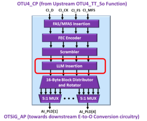
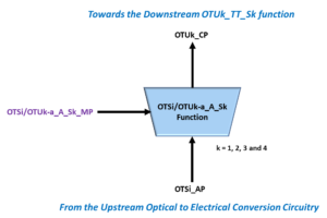
The OTSiG/OTUk_A_Sk Function

The OTSiG/OTUk_A_Sk function is any circuit that takes a group of four electrical lane signals (e.g., the OTSiG signal) and converts this data back into the OTUk signal.

More specifically, the System-Designer will apply this OTSiG group of signals (which are of the OTL3.4 format for OTU3 applications and the OTL4.4 format for OTU4 applications) to the OTSiG_AP Input Interface.

NOTE:  These OTL3.4 or OTL4.4 format signals carry a fully-framed, scrambled OTU3 or OTU4 data stream, often including Forward-Error-Correction.

The OTSiG/OTUk_A_Sk function will then:

  • Multiplex each of these four electrical lanes (of the OTL3.4 or OTL4.4 signals) back into a single OTU3 or OTU4 data stream.
  • Afterward, this function will descramble this OTU3/4 data stream, decode the FEC, and then convert this group of signals into OTUk data, clock, frame-start, and multi-frame-start signals.
  • Finally, this function will output these signals to downstream circuitry (such as the OTUk_TT_Sk function).

Once again, ITU-T G.798 states that the system designer can use this function for either OTU3 or OTU4 rates.

For OTU1 and OTU2 rates, we recommend that the system designer use the OTSi/OTUk_A_Sk function instead.

We discuss the OTSi/OTUk_A_Sk atomic function in another post.

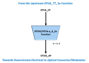
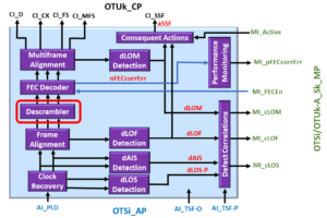
Figure 1 presents a simple illustration of the OTSiG/OTUk_A_Sk function.

OTSiG/OTUk-a_A_Sk Simple Function Diagram

Figure 1, Simple Illustration of the OTSiG/OTUk_A_Sk function.  

Versions of the OTSiG/OTUk_A_Sk Function

ITU-T G.798 defines two versions of this particular function.  Additionally, there are other versions of this function that are not specified by ITU-T G.798.  I list some popular versions of this function below in Table 1.

Table 1, List of Some Popular Versions of the OTSiG/OTUk_A_So function.

Function NameDescriptionComments
OTSiG/OTUk-a_A_SkOTSiG to OTUk Adaptation Sink Function with ITU-T G.709 Standard FEC.Can be used for OTU3 and OTU4 applications ONLY.
OTSiG/OTUk-b_A_SkOTSiG to OTUk Adaptation Sink Function with No FEC. Can be used for OTU3 Applications.
OTSiG/OTUk-v_A_SkOTSiG to OTUk Adaptation Sink Function with Vendor-Specific FECCan be used for OTU3 and OTU4 Applications.

Not specified by ITU-T G.798.

Table 1 shows that the OTSiG/OTUk-a_A_Sk and the OTSiG/OTUk-v_A_Sk functions will compute and decode some sort of FEC field within the backend of each incoming OTUk frame.

However, this table also shows that the OTSiG/OTUk-b_A_Sk version does not support FEC decoding.

Therefore, ITU-T G.798 states that one can use the OTSiG/OTUk-a_A_Sk function for OTU3 and OTU4 applications.  Further, the standard recommends that the user NOT use the OTSiG/OTUk-b_A_Sk function for OTU4 applications.

Network Equipment operating at the OTU4 rate is required to use Forward-Error-Correction.

What Version (of the OTSiG/OTUk_A_Sk function) will we Discuss Throughout this Post?

Throughout this post, we will be discussing the OTSiG/OTUk-a_A_Sk version of this atomic function.

The OTSiG/OTUk-b_A_Sk and OTSiG/OTUk-v_A_Sk atomic functions do everything that the OTSiG/OTUk-a_A_Sk does, except that the -b version does NO FEC Decoding, and the -v version does FEC Decoding differently than what I describe here.

Clueless about OTN? We Can Help!!! Click on the Banner Below to Learn More!!!

Discounts Available for a Short Time!!

So What All Does this Atomic Function Do – In Detail?

The OTSiG/OTUk-a_A_Sk function will accept the 4-lanes of traffic that make up the OTSiG signals from upstream Optical-to-Electrical Conversion circuitry.  This function will perform the following tasks on this incoming data stream.

  • Multiplexing – It will multiplex each of the four lanes of traffic of the OTL3.4 or OTL4.4 signal back into a single OTU3 or OTU4 signal, respectively.
  • Descrambling – It will descramble this incoming data stream.
  • FEC Decoding – The function will decode the FEC field (within the backend of each incoming OTUk frame) and detect and correct most symbol errors within this data stream.
  • Extract the Frame-Start and Multi-Frame Start signals from this incoming data stream.
  • Detect and Flag the following service-affecting defect conditions.
  • Assert the CI_SSF (Server Signal Fail Indicator) output signal (towards the downstream OTUk_TT_Sk function) anytime it declares any service-affecting defect.
  • Output the remaining OTUk data stream, the OTUk clock signal, the Frame-Start, and Multiframe Start signals to downstream circuitry (e.g., typically the OTUk_TT_Sk atomic function).

NOTE:  (*) – Indicates that you need to be a member of THE BEST DARN OTN TRAINING PRESENTATION…PERIOD!!  to see this link.

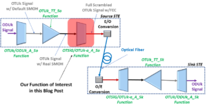
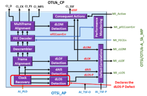
Figure 2 illustrates a Unidirectional Connection that shows where the OTSiG/OTUk-a_A_Sk function “fits in” within a system.

STE to STE Connection - OTSiG/OTUk-a_A_Sk function is highlighted

Figure 2, Illustration of an STE, transmitting an OTUk signal (over optical fiber) to another STE – the OTSiG/OTUk-a_A_Sk function is highlighted.  

Functional Description of this Atomic Function

Let’s now take a closer look at this function.

The OTSiG/OTUk-a_A_Sk functional block diagrams are different for OTU3 applications than for OTU4 applications.  Therefore, we will first walk through the Functional Block Diagram for OTU3 applications.

Afterward, we will do the same for OTU4 applications.

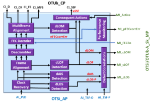
Review of the OTSiG/OTU3-a_A_Sk Functional Block Diagram – OTU3 Applications

Figures 3 and 4 present the Functional Block Diagram of the OTSiG/OTUk-a_A_Sk Atomic Function for OTU3 applications.

NOTE:  The Functional Block Diagrams for this function are rather large and complicated.  Therefore, I had to spread the OTU3 Functional Block Diagram over two figures (Figures 3 and 4).

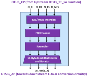
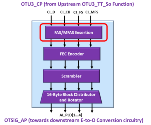
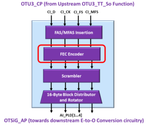
More specifically, Figure 3 presents the OTUk_CP Side of the OTSiG/OTUk-a_A_Sk function, and Figure 4 shows the OTSiG_AP Side of this function.

OTSiG/OTUk-a_A_Sk for OTU3 Applications - OTU3_CP Interface Side

Figure 3, The OTUk_CP Interface Side of the OTSiG/OTUk-a_A_Sk function.

OTSiG/OTUk-a_A_Sk OTU3 Applications - OTSiG_AP Side

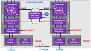
Figure 4, The OTSiG_AP Interface Side of the OTSiG/OTUk-a_A_Sk function.  

Therefore, Figures 3 and 4 show that the OTU3-version of this function contains the following functional blocks.

  • Clock-Recovery and LOS-Detection Block
  • Lane Frame Alignment Block
  • The Lane Alignment Recovery Block
  • Lane-Marker and Delay-Processing Block
  • Elastic Store
  • 16-Byte Block MUX
  • (OTU3) Frame-Alignment and dLOF-Detection Block
  • Descrambler Block
  • FEC Decoder Block
  • Multi-Frame Alignment and dLOM Detection Block

I will briefly discuss each of these functional blocks below.

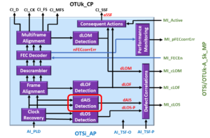
The Clock-Recovery and dLOS-Detection Block (4 for OTU3 Applications)

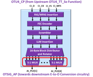
Once our 4-lane Optical Signal passes through the Optical-to-Electrical Conversion (or Demodulator) circuitry, it will be an electrical OTL3.4 signal.  The System-Designer should route each of these OTL3.4 electrical lanes signals to the AI_PLD[1] to AI_PLD[4] inputs to this function.

Once these electrical signals enter the OTSiG/OTU3-a_A_Sk function, they will pass through their corresponding Clock Recovery and dLOS Detection Block.

I show an illustration of the OTSiG_AP Side of the OTSiG/OTU3-a_A_Sk Functional Block Diagram below with the Clock Recovery and dLOS Detection blocks, highlighted below in Figure 5.

OTSiG/OTUk-a_A_Sk - OTU3 Applications - Clock Recovery and dLOS Detection Blocks Highlighted

Figure 5, Illustration of the OTSiG_AP Side of the OTSiG/OTU3-a_A_Sk Functional Block Diagram, with the Clock Recovery and dLOS Detection blocks highlighted.

The OTSiG/OTU3-a_A_Sk function has four Clock Recovery and dLOS Detection Blocks (one for each of the four lanes within the incoming OTL3.4 signal).

The Clock Recovery block is responsible for recovering the clock signal and the data content within a given OTL3.4 lane signal via its corresponding AI_PLD[n] input pin.

Since the OTSiG/OTUk-a_A_So atomic function (at the remote STE) should have scrambled this data stream, each of these incoming lane signals should always have good timing content (or transitions) so that this Clock Recovery block can acquire and extract out both a recovered clock signal and data-stream from each of these incoming lane signals.

Suppose the Clock Recovery block (along with the dLOS Detection Block) were to determine that there is a lengthy absence in signal transitions (within its incoming lane data-stream).  In that case, it will declare the dLOS-P (Loss of Signal – Path) defect for that particular electrical lane.

Please check out the dLOS blog post for more information about the dLOS-P defect condition.

The OTSiG/OTUk-a_A_Sk function will route this recovered clock and data signal (for each electrical lane) to its Lane Frame Alignment block for further processing.

Lane Frame Alignment Block (4 for OTU3 Applications)

The OTSiG/OTU3-a_A_Sk function contains 4 Lane Frame Alignment blocks, one for each Logical (or Electrical) Lane.

I show an illustration of the OTSiG/OTU3-a_A_Sk Functional Block Diagram with the Lane Frame Alignment Blocks highlighted below in Figure 6.

OTSiG/OTUk-a_A_Sk - OTU3 Applications - Lane Frame Alignment Blocks Highlighted

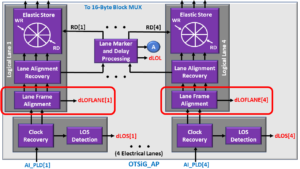
Figure 6, Illustration of the OTSiG/OTU3-a_A_Sk Functional Block Diagram with the Lane Frame Alignment Blocks highlighted.  

In the OTL3.4 post, we mention that (as we create these OTL3.4 lane signals, we purpose “Lane Rotation” as each frame boundary to ensure that each logical lane will carry the FAS-field at some point.

These Lane Frame Alignment blocks aim to acquire FAS-Frame Synchronization with their corresponding Logical Lane signal.  In other words, these Lane Frame Alignment blocks strive to locate each FAS field and maintain a Lane-FAS Frame synchronization with their respective lanes.

Each Lane Frame Alignment block will also declare and clear the dLOFLANE (Loss of Frame – Lane) defect condition as appropriate.  Please see the post on the dLOFLANE defect for more information about this defect condition.

The OTSiG/OTU3-a_A_Sk Function will route these logical lane signals to their own Lane Alignment Recovery Blocks.

Lane Alignment Recovery Block (4 for OTU3 Applications)

The OTSiG/OTU3-a_A_Sk Function contains four Lane Alignment Recovery blocks (one for each Logical Lane it processes).

I show an illustration of the OTSiG/OTU3-a_A_Sk Functional Block Diagram with the Lane Alignment Recovery blocks highlighted below in Figure 7.

OTSiG/OTUk-a_A_Sk - OTU3 Applications - Lane Alignment Recovery Block Highlighted

Figure 7, Illustration of the OTSiG/OTU3-a_A_Sk Functional Block Diagram with the Lane Alignment Recovery blocks highlighted.  

These Lane Alignment Recovery blocks aim to acquire LLM (Logical Lane Marker) Frame Synchronization with its corresponding Logical Lane signal.

The Lane Alignment Recovery blocks also have the following responsibilities:

  • To report the LLM value, within its logical lane, to the Lane Marker and Delay Processing block, and
  • To alert the Lane Marker and Delay Processing block, the instant that (the Lane Alignment Recovery block) detects and receives the LLM fields within its incoming Logical Lane data stream.

Four blocks will work in tandem with the Lane Marker and Delay Processing block to declare and clear the dLOL (Loss of Lane Alignment) defect condition.

Please see the blog post on the dLOL defect to learn more about this defect condition.

Once a given Logical Lane signal passes through the Lane Alignment Recovery block, the OTSiG/OTU3-a_A_Sk function will route these signals to the Elastic Store block for further processing.

Lane Marker and Delay Processing Block (1 for OTU3 Applications)

The OTSiG/OTU3-a_A_Sk function only has one Lane Marker and Delay Processing block.

I illustrate the OTSiG/OTU3-a_A_Sk Functional Block Diagram with the Lane Marker and Delay Processing Block highlighted below in Figure 8.

OTSiG/OTUk-a_A_Sk Function - OTU3 Applications - Lane Marker and Delay Processing Block Highlighted

Figure 8, Illustration of the OTSiG/OTU3-a_A_Sk Functional Block Diagram with the Lane Marker and Delay Processing Block highlighted.

The Lane Marker and Delay Processing block have the following responsibilities:

  • To declare and clear the dLOL defect condition.
  • To compensate for skew between each of the four Logical Lanes.
  • And to ensure that each Logical Lane will be processed in the correct order/sequence, the OTSiG/OTU3-a_A_Sk function will successfully reconstruct the original OTU3 data stream.
  • To ensure that each Logical Lane has its unique value for the LLM ID.

To accomplish this, the Lane Marker and Delay Processing block will work in tandem with each of the 4 Lane Alignment Recovery blocks and the Elastic Store blocks.

In general, the Lane Marker and Delay Processing block will use the “LLM Received” information from each of the 4 Lane Alignment Recovery blocks to determine the amount of skew between them.

The Lane Marker and Delay Processing block will use the Elastic Store blocks to buffer and delay all of the “faster” Logical lanes until the “slowest” (or most delayed) Logical Lane “catches up.”

Once this slowest Logical Lane catches up, the Lane Marker and Delay Processing block will allow the 16-Byte MUX to read out the contents of the logical lane data from each of the 4 Elastic Store blocks.

The Elastic Store Block (4 for OTU3 Applications)

The OTSiG/OTU3-a_A_Sk function contains four Elastic Store blocks (one for each Logical Lane).

I illustrate the OTSiG/OTU3-a_A_Sk Functional Block Diagram with the Elastic Store blocks highlighted below in Figure 9.

OTSiG/OTUk-a_A_Sk Function Block Diagram - OTU3 Applications - Elastic Store Blocks Highlighted

Figure 9, Illustration of the OTSiG/OTU3-a_A_Sk Functional Block Diagram with the Elastic Store blocks highlighted.  

The Elastic Store block is an array of buffers (or storage) within the four logical lanes.   The OTSiG/OTU3-a_A_Sk function will load the contents of each Logical Lane data stream into this buffer as it arrives at this block.

However, the Lane Marker and Delay Processing Block will determine how long this data will remain in this Elastic Store block before it travels downstream towards the 16-Byte Block MUX.

The Lane Marker and Delay Processing block will control exactly when this Logical Lane data is read out from each of the 4 Elastic Store blocks to compensate for skew between each Logical Lanes.

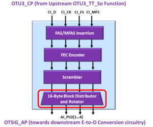
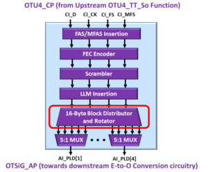
16-Byte Block MUX (1 for OTU3 Applications)

The OTSiG/OTU3-a_A_Sk function contains one 16-Byte Block MUX.

I show an illustration of the OTUk_CP Interface Side of the OTSiG/OTU3-a_A_Sk Functional Block Diagram, with the 16-Byte Block MUX highlighted below in Figure 10.

OTSiG/OTUk-a_A_Sk Functional Block Diagram - OTU3 Applications - 16 Byte Block MUX Highlighted

Figure 10, Illustration of the OTSiG/OTU3-a_A_Sk Functional Block Diagram (OTUk_CP Side) with the 16-Byte Block MUX Highlighted.

The purpose of the 16 Byte Block MUX is to read out the contents of each of the Elastic Store blocks (with each of the four Logical Lanes) and to multiplex this data into a single OTU3 data stream.

The 16 Byte Block MUX (as its name implies) will read out data, 16 bytes at a time, from each of the four Elastic Store blocks.  Additionally, the 16-Byte Block MUX will execute these READ Operations under the direction of the Lane Marker and Delay Processing block.

The 16 Byte Block MUX, the Lane Marker, and Delay Processing Blocks, and the Lane Alignment Recovery blocks will work together to:

  • Compensate for skew between each of the Logical Lanes, and
  • Properly multiplex and (reassemble) a full-blown, serial OTU3 data stream.

After the 16-Byte Block MUX has reassembled this OTU3 data stream, it will route this data stream over to the (OTU3) Lane Frame Alignment and dLOF Detection Block for further processing.

Has Inflation got You Down? Our Price Discounts Can Help You Fight Inflation and Help You Become an Expert on OTN!!! Click on the Banner Below to Learn More!!!

Corporate Discounts Available!!!

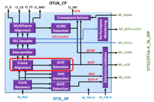
(OTU3) Frame Alignment and dLOF Detection Blocks

Once our data stream has reached the Frame Alignment and dLOF Detection Block, we are no longer working with OTL3.4 Logical Lanes.  The 16 Byte Block MUX has multiplexed all four logical lanes into a single OTU3 data stream.

I illustrate the OTSiG/OTU3-a_A_Sk Functional Block Diagram with the Frame Alignment and dLOF Detection Blocks highlighted below in Figure 11.

OTSiG/OTUk-a_A_Sk Functional Block Diagram - OTU3 Applications - OTU3 Frame Alignment and dLOF Detection Block Highlighted

Figure 11, Illustration of the OTSiG/OTU3-a_A_Sk Functional Block Diagram with the Frame Alignment and dLOF Detection Blocks highlighted.  

The only question now is:  Did we multiplex the four OTL3.4 Logical Lanes together correctly?

If we were to assume all of the following conditions to be true:

  • That none of the four Frame Alignment Blocks (within the OTSiG/OTU3-a_A_Sk function) were declaring the dLOFLANE defect condition, and
  • The Lane Marker and Delay Processing block did not report any issues with Excessive Skew.

Then the 16-Byte Block MUX should have correctly and successfully multiplexed these four Logical Lanes into a single valid OTU3 data stream.

However, the (OTU3) Frame Alignment and dLOF Detection Block can serve as an additional check to ensure that our multiplexing operation is successful.  This is why I’ve listed this particular functional sub-block as “Optional.”

This sub-block aims to acquire and maintain OTUk-FAS Frame Synchronization with this newly combined OTU3 data stream.  If this block fails to obtain and maintain synchronization with the incoming FAS frames, it will declare the dLOF (Loss of Frame) defect condition.

Please see the dLOF (Loss of Frame) blog post for more information on how the Frame Alignment and dLOF Detection Block declare and clear the dLOF defect condition.

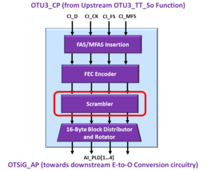
Once this OTU3 data stream leaves the Frame Alignment and dLOF Detection Block, it will enter the Descrambler Block for further processing.

Descrambler Block

In the OTSiG/OTUk-a_A_So blog post, I mentioned that the OTSiG/OTUk-a_A_So function would scramble the content of each outbound OTUk frame.

That function will scramble all bytes (within each OTUk frame) except for the FAS fields.  This function will even scramble the MFAS field as well.

The purpose of the Descrambler block is to restore the content of each OTUk frame to its original state before being scrambled by the remote STE.

I show an illustration of the OTSiG/OTU3-a_A_Sk Functional Block Diagram with the Descrambler block highlighted below in Figure 12.

OTSiG/OTUk-a_A_Sk Functional Block Diagram - OTU3 Appilcations - Descrambler Block Highlighted

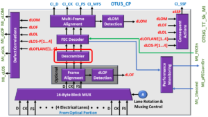
Figure 12, Illustration of the OTSiG/OTU3-a_A_Sk Functional Block Diagram with the Descrambler block highlighted.  

In the OTSiG/OTUk-a_A_So function, we scrambled the contents of OTUk frame, using the polynomial generating equation of 1 + x + x3 + x12 + x16.

Therefore, the Descrambler block (within this function) will descramble the incoming OTUk data-stream (again) using the polynomial generating equation of 1 + x + x3 + x12 + x16.

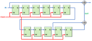
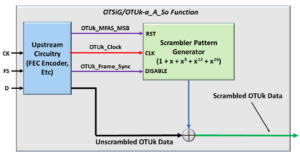
I show a simple diagram of how one can implement the Descrambler within their OTSiG/OTUk-a_A_Sk function design below in Figure 13.

Descrambler Block Level Diagram with OTSiG/OTUk_A_Sk Function

Figure 13, High-Level Block Diagram of the Frame Synchronous Descrambler.

I discuss the Descrambler function and requirements in greater detail in another post.

Once the OTU3 data stream passes through and exits the Descrambler block, it will proceed onto the FEC Decoder block for further processing.

FEC Decoder Block

I illustrate the OTSiG/OTU3-a_A_Sk Functional Block Diagram with the FEC Decoder block highlighted below in Figure 14.

OTSiG/OTUk-a_A_Sk Functional Block Diagram - OTU3 Applications - FEC Decoder Block Highlighted

Figure 14, Illustration of the OTSiG/OTU3-a_A_Sk Functional Block Diagram with the FEC Decoder block highlighted.  

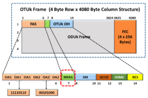
The OTSiG/OTU3-a_A_So function (at the remote STE) is responsible for performing FEC (Forward-Error-Correction) Encoding.

This means that this function computed a FEC Code and inserted that code into a 4-row x 128-byte column field at the backend of each OTU3 frame, as shown below in Figure 15.

OTUk Frame with FEC Field highlighted

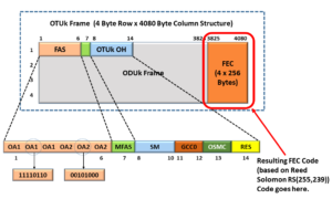
Figure 15, Illustration of the OTUk Frame Format with the FEC Field Highlighted

The purpose of the FEC Decoder (within the OTSiG/OTU3-a_A_Sk function) is to parse through the incoming OTU3 data stream and (by using the contents of the FEC-field) detect and correct most symbol errors within this data stream.

The FEC Decoder block will count and tally any occurrences of Symbol errors (within the incoming OTU3 data stream.).  It will report this information to System Management via the MI_pFECcorrErr output (via the OTSiG/OTU3-a_A_Sk_MP Interface).

I discuss Forward-Error-Correction in much greater detail in another post.

Multi-Frame Alignment and dLOM Detection Block

Once the incoming OTU3 data stream passes through the FEC Decoder block, the OTSiG/OTU3-a_A_Sk function will route this signal to the Multi-Frame Alignment and dLOM Detection blocks.

I illustrate the OTSiG/OTU3-a_A_Sk Function Block Diagram with the Multi-Frame Alignment and dLOM Detection block, highlighted below in Figure 16.

OTSiG/OTUk-a_A_Sk Functional Block Diagram - Multi-Frame Alignment - dLOM Detection Blocks Highlighted

Figure 16, Illustration of the OTSiG/OTU3-a_A_Sk Functional Block Diagram with the Multi-Frame Alignment and dLOM Detection Block highlighted.  

The Mult-Frame Alignment block will parse through and check the contents of the MFAS field within the incoming OTU3 data stream.  The Multi-Frame Alignment block will check the contents of this data stream to see if it (and the dLOM Detection Block) should declare or clear the dLOM (Loss of Multi-Frame Alignment) defect condition.

Please see the blog post on the dLOM defect for more information on how the Multi-Frame Alignment block will declare and clear the dLOM defect condition.

Removal of the FAS, MFAS, and FEC Fields from the incoming OTU3 Data-stream

The Frame-Alignment block will drive the CI_FS (Frame-Start) output of the OTUk_CP Interface, HIGH for one CI_CK (Clock Signal) period, each time it detects the FAS field within its incoming OTUk data-stream.

Likewise, the Multi-Frame Alignment block will drive the CI_MFS (Multi-Frame Start) output of the OTUk_CP Interface, HIGH, for one CI_CK (Clock Signal) period each time it receives an MFAS byte with the value of 0x00.

The Frame-Alignment and Multi-Frame Alignment block will also remove the FAS and MFAS fields from the OTUk data stream (before it outputs this data stream via the CI_D output of the OTUk_CP Interface).

From this point on, the CI_FS and CI_MFS signals will now carry the framing and multi-framing alignment information downstream towards the OTUk_TT_Sk atomic function.

The FEC Decoder block will also remove the contents of the FEC field from the OTUk data stream before it outputs this data via the CI_D output pin.

We have briefly covered the OTSiG/OTUk-a_A_Sk function description for OTU3 applications.  Let’s move on and discuss this atomic function for OTU4 applications.

Clueless about OTN? We Can Help!!! Click on the Banner Below to Learn More!!!

Corporate Discounts Available!!!

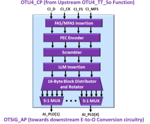
Review of the OTSiG/OTU4-a_A_Sk Functional Block Diagram – OTU4 Applications

I present the Functional Block Diagram of the OTSiG/OTUk-a_A_Sk Atomic Function for OTU4 Applications below in Figures 14, 15, and 16.

NOTE:  The Functional Block Diagrams for this function are rather large and complicated.  Therefore, I had to spread the OTU3 Functional Block Diagram over three figures (Figures 17, 18, and 19).

Figure 17 presents the OTUk_CP Side of the OTSiG/OTUk-a_A_Sk function.

OTSiG/OTUk-a_A_Sk Functional Block Diagram - OTU4 Applications - OTUk_CP Interface Side

Figure 17, Illustration of the Functional Block Diagram of the OTSiG/OTU4-a_A_Sk Atomic Function – The OTUk_CP Interface Side

Additionally, Figure 18 presents the Middle Portion of the OTSiG/OTUk-a_A_Sk function.

OTSiG/OTUk-a_A_Sk Function - OTU4 Applications - Middle Portion

Figure 18, Illustration of the Functional Block Diagram of the OTSiG/OTU4-a_A_Sk Atomic Function – The Middle Portion

Finally, Figure 19 shows the OTSiG_AP Side of this function.

OTSiG/OTUk-a_A_Sk Functional Block Diagram - OTU4 Applications - OTSiG_AP Interface Side

Figure 19, Illustration of the Functional Block Diagram of the OTSiG/OTU4-a_A_Sk Atomic Function – The OTSiG_AP Interface Side

Hence, these figures show that the OTU4 version of this function contains the following functional sub-blocks.

  • The Clock Recovery and dLOS Detector Block
  • The 1/5 Bit De-Interleaver Blocks
  • The Lane Frame Alignment Blocks
  • The Lane Alignment Recovery Blocks
  • The LLM Removal Block
  • The Lane Marker and Delay Processing Block
  • The Elastic Store Blocks
  • The 16-Byte Block MUX
  • The (OTU4) Frame Alignment – dLOF Detection Block
  • The Descrambler Block
  • The FEC Decoder Block
  • The Multi-Frame Alignment and dLOM Detection Block

I will discuss some of these Functional blocks below.  Please note that some of these blocks are identical to what I’ve presented for OTU3 applications.  I will note that whenever I come across those functional sub-blocks.

The Clock Recovery and dLOS Detection Block (4 for OTU4 Applications)

Please see the description for the Clock Recovery and dLOS Detection Block above for OTU3 applications.

The 1/5 Bit De-Interleaver Blocks (4 for OTU4 Applications)

Once the OTL4.4 signal passes through the Clock Recovery block, it will proceed onto the 1/5 Bit De-Interleaver blocks for further processing.

The OTSiG/OTU4-a_A_Sk function contains four of these 1/5 Bit De-Interleaver Blocks.

I illustrate the OTSiG/OTU4-a_A_Sk Functional Block Diagram with the 1/5 Bit De-Interleaver blocks highlighted below in Figure 20.

OTSiG/OTUk-a_A_Sk Functional Block Diagram - OTU4 Applications - 1/5 Bit De-Interleavers Highlighted

Figure 20, Illustration of the OTSiG/OTU4-a_A_Sk Functional Block Diagram with the 1/5 Bit De-Interleavers blocks highlighted.

Each lane (within the incoming OTL4.4 signal) will pass through its own 1/5 Bit De-Interleaver Blocks.

Each of these 1/5 Bit De-Interleaver blocks will bit-wise demultiplex five logical lanes of traffic from each incoming electrical lane.  Therefore, when the four lanes (within an OTL4.4 signal) pass through their own 1/5 Bit De-Interleaver blocks, they will demultiplex this OTL4.4 signal into 20 logical lanes of traffic.

The Lane Frame Alignment Block (20 for OTU4 Applications)

Please see the description for the Lane Frame Alignment Block above for OTU3 applications.  Please note that the OTSiG/OTU4-a_A_Sk function will have 20 blocks, whereas the OTU3 version only has 4.

The Lane Alignment Recovery Blocks (20 for OTU4 Applications)

Please see the description for the Lane Alignment Recovery Block above for OTU3 applications.  Please note that the OTSiG/OTU4-a_A_Sk function will have 20 blocks, whereas the OTU3 version only has 4.

The LLM (Logical Lane Marker) Removal Blocks (20 for OTU4 Applications)

Once each Logical Lane signal passes through and exits their Lane Alignment Recovery block, they will proceed to their respective LLM Removal Blocks.

I illustrate the OTSiG/OTU4-a_A_Sk functional block diagram with the LLM Removal Blocks highlighted below in Figure 21.

OTSiG/OTUk-a_A_Sk Functional Block Diagram - OTU4 Applications - LLM Removal Blocks Highlighted

Figure 21, Illustration of the OTSiG/OTU4-a_A_Sk Functional Block Diagram with the LLM Removal Blocks highlighted.

If you recall, from our OTL4.4 post, the OTSiG/OTU4-a_A_Sk function (at the remote STE) will “borrow” the 3rd OA2 byte (within the FAS field of each outbound OTU4 frame) and use it as the LLM (Logical Lane Marker) field.

I illustrate the OTU4 Frame format with this LLM (and borrowed OA2) byte-field highlighted below in Figure 22.

OTU4 Frame with 3rd OA2 Byte being used as the OTL4.4 Logical Lane Marker

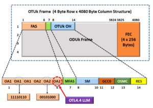
Figure 22, Illustration of an OTU4 Frame with the LLM Field location highlighted.  

The purpose of the LLM Removal (in this function) is to remove the LLM field from this 3rd OA2 byte-field and (effectively) give this byte back to the transport system by restoring its value to 0x28.

Once the Logical Lane data stream passes through to the LLM Removal Block, it will proceed to the Elastic Store block for further processing.

The Lane Marker and Delay Processing Block (1 for OTU4 Applications)

Please see the description for the Lane Marker and Delay Processing Block above for OTU3 applications.  Please note that the Lane Marker and Delay Processing Block within the OTSiG/OTU4-a_A_Sk function will be working with 20 sets of the Lane Alignment Recovery and Elastic Store Blocks for Skew Compensation purposes.

The Elastic Store Blocks (20 for OTU4 Applications)

Please see the description for the Elastic Store Block above for OTU3 applications.  Please note that the OTSiG/OTU4-a_A_Sk function will have 20 blocks, whereas the OTU3 version only has 4.

The 16-Byte Block MUX

Please see the description for the Elastic Store Block above for OTU3 applications.

The (OTU4) Frame Alignment – dLOF Detection Blocks

Please see the description for the Elastic Store Block above for OTU3 applications.

The Descrambler Blocks

Please see the description for the Elastic Store Block above for OTU3 applications.

The FEC Decoder Block

Please see the description for the Elastic Store Block above for OTU3 applications.

The Multi-Frame Alignment – dLOM Detection Blocks

Please see the description for the Elastic Store Block above for OTU3 applications.

Consequent Actions Blocks

I illustrate the OTSiG/OTU4-a_A_Sk function with the Consequent Actions blocks highlighted below in Figure 23.

OTSiG/OTUk-a_A_Sk Consequent Actions Equation Highlighted - OTU3 Applications

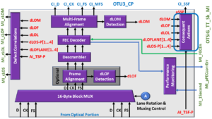
Figure 23, Illustration of the OTSiG/OTU4-a_A_Sk function with the Consequent Actions block highlighted.  

In most cases, the System Designer will realize the Consequent Actions Block via digital logic circuitry that will assert the CI_SSF (Server Signal Fail) output (of the OTUk_CP Interface) anytime the OTSiG/OTUk-a_A_Sk function declares the following defect conditions.

NOTE:  Whenever this function asserts the CI_SSF output signal, it also asserts the CI_SSF input to the downstream OTUk_TT_Sk function.

The Consequent Action Equation for the OTSiG/OTUk-a_A_Sk Atomic Function

ITU-T G.798 lists the following Consequent Actions Equation below:

  • aSSF ⇐ dLOF or dLOM or ∑dLOS-P[i] or dLOL or ∑dLOFLANE[j] or AI_TSF

This equation means that the OTSiG/OTUk-a_A_Sk function should assert the aSSF (and, in turn, drive the CI_SSF output pin HIGH) if any of the following conditions are TRUE:

  • The upstream Optical Circuitry is asserting the AI_TSF-P input signal to this function, or
  • If the OTSiG/OTUk-a_A_Sk function is declaring any of the following defect conditions:

Defect Correlation

If you wish to learn more about Defect Correlation and how you should interpret it, please see the Defect Correlation Post.

ITU-T G.798 specifies the following correlation equations for each OTSiG/OTUk-a_A_Sk function-related defect.

  • cLOS ⇐ ∑dLOS-P[i] and (NOT AI_TSF-P)
  • cLOL ⇐ (dLOL or ∑dLOFLANE[j]) and (NOT ∑dLOS-P[i]) and (NOT AI_TSF-P)
  • cLOF ⇐ dLOF and (NOT ∑dLOS-P[i]) and (NOT AI_TSF-P)
  • cLOM ⇐ dLOM and (NOT dLOF) and (NOT ∑dLOS-P[i]) and (NOT AI_TSF)

I will briefly explain what each of these equations means below.

cLOS ⇐ ∑dLOS-P[i] and (NOT AI_TSF-P)

This equation means that the OTSiG/OTUk_A_Sk function must declare the dLOS defect (and assert the cLOS output pin) if the Clock Recovery and dLOS Detection Circuitry declares the dLOS-P signal within any one of the four electrical lane signals.

This equation also states that the OTSiG/OTUk_A_Sk function must NOT declare the dLOS (and assert the cLOS output pin) if the upstream Optical Circuitry is also asserting the AI_TSF-P input signal (to this function).

cLOL ⇐ (dLOL or ∑dLOFLANE[j]) and (NOT ∑dLOS-P[i]) and (NOT AI_TSF-P)

This equation means that the OTSiG/OTUk_A_Sk function should only declare the dLOL defect (and assert the cLOL output pin) if either of the following conditions is TRUE:

  • If the Lane Marker and Delay Processing block is declaring the dLOL defect, OR
  • If at least one of the 4 or 20 Logical Lanes declare the dLOFLANE defect conditions.

However, this equation also states that the function CANNOT declare the dLOL defect (and drive the cLOL output pin HIGH) if either of the following conditions is TRUE:

  • At least one Clock Recovery and dLOS Detection circuit is also declaring the dLOS-P defect conditions with any one of the four electrical lane signals, OR
  • The upstream circuitry currently asserts the AI_TSF-P input pin (to this function).

cLOF ⇐ dLOF and (NOT ∑dLOS-P[i]) and (NOT AI_TSF-P)

This equation means that the OTSiG/OTUk-a_A_Sk function should only declare the dLOF defect (and assert the cLOF output pin) if the Frame Alignment block and the dLOF Detection blocks declare the dLOF defect condition.

However, this equation also states that the function CANNOT declare the dLOF defect (and drive the cLOF output pin HIGH) if any of the following conditions are TRUE:

  • At least one Clock Recovery and dLOS Detection circuit is also declaring the dLOS-P defect conditions with any one of the four electrical lane signals, OR
  • The upstream optical circuitry is currently asserting the AI_TSF-P input pin (to this function).

cLOM ⇐ dLOM and (NOT dLOF) and (NOT ∑dLOS-P[i]) and (NOT AI_TSF-P)

This equation means that the OTSiG/OTUk-a_A_Sk function should only declare the dLOM defect (and assert the cLOM output pin) if the Multi-Frame Alignment block and the dLOM Detection blocks declare the dLOM defect condition.

However, this equation also states that the function CANNOT declare the dLOM defect (and drive the cLOM output pin HIGH) if any of the following conditions are TRUE:

  • The Frame Alignment and dLOF Detection blocks are also declaring the dLOF defect condition, or
  • If at least one Clock Recovery and dLOS Detection block is declaring the dLOS defect with its electrical lane signal, or
  • The Optical upstream circuitry is currently asserting the AI_TSF-P input pin (to this function).

Performance Monitoring

ITU-T G.798 requires that the OTSiG/OTUk-a_A_Sk Function tally and report the following Performance Monitoring parameter to System Management:

pFECcorrErr ⇐ ∑nFECcorrErr

In other words, we expect the OTSiG/OTUk-a_A_Sk function to tally and report each time the FEC Decoder block corrects an errored symbol within the incoming OTU3 or OTU4 data stream.

Pin Description

I list the Input/Output Pin Description for the OTSiG/OTUk-a_A_Sk Atomic Function below in Table 2.

Table 2, Pin Description for the OTSiG/OTUk-a_A_Sk Atomic Function

SignalTypeDescription
OTSiG Access Point - Interface
AI_PLD[1...4]InputOTSiG Adaptation Information - PLD (Payload) Input Ports 1 through 4:
The user is expected to apply a 4-lane electrical signal to these inputs. This four-lane signal should be an OTL3.4 type of signal for OTU3 applications and an OTL4.4 type of signal for OTU4 applications.

In most cases, this 4-lane electrical signal will have just recently been converted from the optical, back into the electrical format.

The OTSiG/OTUk-a_A_Sk function will convert the 4-lane OTL3.4 signal back into a single-composite OTU3 signal. Likewise, this function will also convert the 4-lane OTL4.4 signal back into a single-composite OTU4 signal.
OTUk - Characteristic Information
CI_DOutputOTUk Characteristic Information - Data Output:
The OTSiG/OTUk-a_A_Sk function will output the OTUk data via this output. This OTUk data will contain all of the following portions of the OTUk frame.
- OTUk-SMOH (Section Monitoring Overhead) data
- All remaining OTUk payload data (e.g., the ODUk/OPUk data).

This data will not include the FAS, MFAS nor FEC fields, however.

Data that is output via this signal, will be aligned with one of the clock edges of the CI_CK clock output signal. The system designer will typically route this signal to the CI_D input to the downstream OTUk_TT_Sk function.
CI_CKOutputOTUk Characteristic Information - Clock Output:
As the OTUk CP Interface outputs data via the CI_D, CI_FS, CI_MFS and CI_SSF outputs; all of this data will be updated to one of the clock edges of this clock output signal.
CI_FSOutputOTUk Characteristic Information - Frame Start Output:
The OTUk_CP interface will pulse this output signal HIGH whenever the OTUk_CP interface outputs the very first bit (or byte) of a new OTUk frame, via the CI_D output.

This output signal will pulse HIGH once for each OTUk frame.
CI_MFSOutputOTUk Characteristic Information - Multi-Frame Start Output:
The OTUk_CP Interface will pulse this output signal HIGH whenever the OTUk_CP Interface outputs the very first bit (or byte) of a new OTUk multi-frame, via the CI_D output.

This output signal will pulse HIGH once for each OTUk Multi-frame (or once each 256 OTUk fraeme
CI_SSFOutputOTUk Characteristic Information - Server Signal Failure Output:
The OTUk_CP interface will assert this signal anytime the OTSiG/OTUk-a_A_Sk function is declaring a service-affecting defect with the data that it is receiving via the AI_D input.

The OTUk_CP Interface will assert this output signal, whenever the OTSiG/OTUk-a_A_Sk function is declaring any of the followiong defects.
- dLOF
- dLOM
- dLOL
- dLOFLANE (within any of the 4 or 20 logical lanes)
- dLOS-P (within any of the four electrical lanes).
OTSiG/OTUk-a_A_Sk_MP Management Interface
MI_FECEnInputOTSiG/OTUk-a_A_Sk FEC Decoding Enable/Disable Input:
This input pin permits the function user to either enable or disable FEC Decoding within the OTSiG/OTUk-a_A_Sk function.

Setting this input HIGH enables FEC Decoding.

Setting this input LOW disables FEC Decoding.

NOTE: This input does not exist for OTU4 applications.
MI_1SecondInputManagement Interface - One Second Clock Input:
The user is expeced to supply a clock signal, which has a frequency of 1Hz to this input.

The Performance Monitoring portion of the OTSiG/OTUk-a_A_Sk function will use this clock signal as its timing reference for tallying and reporting the various One-Second Performance Monitoring parameters.
MI_cLOFOutputManagement Interface - Loss of Frame (Correlated) Output Indicator:
This output pin indicates if the OTSiG/OTUk-a_A_Sk function is currently declaring the dLOF defect.

If this output pin is LOW, then it indicates that the function is NOT currently declaring the dLOF defect condition.

Conversely, if this output pin is HIGH, then it indicates that the function is currently declaring the dLOF defect condition.

Please the blog post for dLOF defect, to learn more about how the OTSiG/OTUk-a_A_Sk function declares and clears the dLOF defect condition.
MI_cLOMOutputManagement Interface - Loss of Multiframe (Correlated) Output Indicator:
This output pin indicates if the OSiG/OTUk-a_A_Sk function is currently declaring the dLOM defect condition.

If this input pin is LOW, then it indicates that the function is NOT currently declaring the dLOM defect condition.

Conversely, if this input pin is HIGH, then it indicates that this function is currently declaring the dLOM defect condition.

Please see the dLOM blog post, for more information on how the OTSiG/OTUk-a_A_Sk function declares and clears the dLOM defect condition.
MI_cLOLOutputManagement Interface - Loss of Lane Alignment (Correlated) Output Indicator:
This output pin ndicates if the OTSiG/OTUk-a_A_Sk function is currently declaring the dLOL defect.

If this output pin is LOW, then it indicates that the function is NOT currently declaring the dLOL defect condition.

Conversely, if this output pin is HIGH, then it indicates that the function is currently declaring the dLOL defect condition.

Please see the dLOL blog post for more information on how the OTSiG/OTUk-a_A_Sk function declares and clears the dLOL defect condition.
MI_cLOSOutputManagement Interface - Loss of Signal (Correlated) Defect Output Indicator:
This output indicates if the OTSiG/OTUk-a_A_Sk function is currently declaring the dLOS defect condition.

If this output pin is LOW, then it indicates that the function is NOT currently declaring the dLOS defect condition.

Conversely, if this output pin is HIGH, then it indicates that the function is currently declaring the dLOS defect condition.

Please see the dLOS blog post, for more information on how the OTSiG/OTUk-a_A_Sk function declares and clears the dLOS defect condition.
MI_pFECcorrErrOutputManagement Interface - FEC Correlated Error Count Output:
This output port reflects the number of symbol errors that the OTSiG/OTUk-a_A_Sk function (via the FEC Decoder) has corrected.

This is a Performance Monitoring feature within the OTSiG/OTUk-a_A_Sk function.

NOTE: This outputpin is INACTIVE if the MI_FECEn input pin is set LOW (to disable the FEC Decoder).

Clueless about OTN? We Can Help!! Click on the Banner Below to Learn More!!

Discounts Available for a Short Time!!!

Other OTN-Related Posts

Click on the Image below to see more OTN-Related Posts on this blog.

OTN Related Blog

OTN Related Topics within this Blog

OTN Related Topics within this Blog General Topics Consequent Equations - What are they and How can you use them? ...

What is the OTSiG/OTUk_A_So Function?

This blog post briefly describes the OTSiG/OTUk-a_A_So Atomic Function. The main purpose of this Atomic Function is to either convert an OTU3 data-stream into the OTL3.4 format, or to convert the OTU4 data-stream into the OTL4.10 or OTL4.4 format.

What is the OTSiG/OTUk_A_So Atomic Function?

The expression:  OTSiG/OTUk_A_So is an abbreviation for the term:  Optical Tributary Signal Group to OTUk Adaptation Source Function.

This blog post will briefly describe the OTSiG/OTUk_A_So set of atomic functions.

Changes in Terminology

Before we proceed on with this post, we need to cover some recent changes in terminology.  Before the June 2016 Version of ITU-T G.709, the standard documents referred to this particular atomic function as the OPSM/OTUk_A_So function.

However, the standards committee has recently decided to change the wording from using the term OPSM (Optical Physical Section Multilane) to using the word OTSiG (for Optical Tributary Signal Group).

For completeness, I will tell you that ITU-T G.709 defines the term OTSiG as:

The set of OTSi signals that supports an OTU.”

Therefore, where we used the OTSi/OTUk_A_So and OTSi/OTUk_A_Sk functions for “single-lane” applications, we will use the OTSiG/OTUk_A_So and OTSiG/OTUk_A_Sk functions for “multi-lane” applications.

In summary, to “speak the same language,” as does the standard committee, we will call this atomic function the OTSiG/OTUk_A_So atomic function.

Likewise, in another post, we will now call (what we used to call the OPSM/OTUk_A_Sk function) the OTSiG/OTUk_A_Sk function.

I have created another post that provides documentation of the relationships between some old (now obsolete) terms and the new (and approved) ones that our standard committee is currently using.

A Little More about Multi-Lane Interfaces for OTU3 and OTU4 Applications

First, we only use the OTSiG/OTUk_A_So and OTSiG/OTUk_A_Sk functions for OTU3 and OTU4 Multi-Lane applications.

We will use the OTSiG/OTUk_A_So function for OTU3 applications to model circuitry that demultiplexes an OTU3 signal into a four-lane signal (e.g., an OTL3.4 signal).  ITU-T G.709 defines the OTL3.4 signal as an approach to transporting OTU3 traffic over 4-lanes in parallel.

Likewise, we will use the OTSiG/OTUk_A_So function for OTU4 applications to model circuitry that demultiplexes (and multiplexes) an OTU4 signal into a four-lane signal (e.g., an OTL4.4 signal).  ITU-T G.709 also defines the OTL4.4 signal as an approach to transporting OTU4 traffic over 4-lanes in parallel.

Please see the blog posts for the OTL3.4 and OTL4.4 Interfaces for more information on these topics.

The OTSiG/OTUk_A_So Function

The OTSiG/OTUk_A_So function is any circuit that takes an OTUk data-stream, clock, frame-start, and multi-frame start signals and:

  • converts this data into a combined, scrambled data stream, which (in some cases) contains a FEC (Forward-Error-Correction) field, and
  • demultiplexes this data into four electrical lanes, each of which can be readily converted into the optical format (at the output pins of this function).

Once again, ITU-T G.798 states that the system designer can use this function only for the OTU3 or OTU4 rates.

For OTU1 and OTU2 rates, we recommend that the system designer use the OTSi/OTUk_A_So function instead.

We discuss the OTSi/OTUk_A_So atomic function in another post.

Figure 1 presents a simple illustration of the OTSiG/OTUk_A_So function.

OTSiG/OTUk-a_A_So Atomic Function - Simple Drawing

Figure 1, Simple Illustration of the OTSiG/OTUk_A_So function.

ITU-T G.798 defines two versions of this particular function.   Additionally, there are other versions of this function that are not specified by ITU-T G.798.  I list some popular versions of this function below in Table 1.

Table 1, List of Some Popular Versions for the OTSiG/OTUk_A_So function.  

Function NameDescriptionComments
OTSiG/OTUk-a_A_SoOTSiG to OTUk Adaptation Source Function with ITU-T G.709 Standard FEC.Can be used for OTU3 and OTU4 applications ONLY.
OTSiG/OTUk-b_A_SoOTSiG to OTUk Adaptation Source Function with No FECCan only be used for OTU3 Applications.

Cannot be used for OTU4 applications.
OTSiG/OTUk-v_A_SoOTSiG to OTUk Adaptation Source Function with Vendor-Specific FECCan be used for OTU3 and OTU4 Applications.

Not specified by ITU-T G.798.

Table 1 shows that the OTSiG/OTUk-a_A_So and the OTSiG/OTUk-v_A_So functions will compute and append some sort of FEC field to the back-end of each outbound OTUk frame.

However, this table also shows that the OTSiG/OTUk-b_A_So version does not generate the FEC field.

Consequently, ITU-T G.798 states that one can use the OTSiG/OTUk-a_A_So and OTSiG/OTUk-v_A_So functions for OTU3 and OTU4 applications.  The standard also recommends that the user NOT use the OTSiG/OTUk-b_A_So function for OTU4 applications.

The OTU4 rate requires the use of Forward-Error-Correction.

What Version will we Discuss Throughout this Post?

Throughout this post, we will be discussing the OTSiG/OTUk-a_A_So version of this atomic function.

The OTSiG/OTUk-b_A_So and OTSiG/OTUk-v_A_So atomic functions do everything that the OTSiG/OTUk-a_A_So does, except that the -b version does NO FEC Encoding, and the -v version does FEC Encoding differently than what I describe here.

Stuck at Home? You Can Be an Expert on OTN Before You Return to Your Office!!! Click on the Banner Below to Learn More!!

Corporate Discounts Available!!!

So What All Does this Atomic Function Do?

The OTSiG/OTUk-a_A_So function will accept the OTUk data-stream, OTUk clock signal, frame-start signal, and multi-frame start signals via the CI_D, CI_CK, CI_FS, and CI_MFS inputs (of this function) respectively, and it will perform the following tasks.

  • It will insert the FAS and MFAS fields into the outbound OTUk data stream (coincident with whenever the upstream OTUk_TT_So function asserts the CI_FS and CI_MFS inputs, respectively).
  • This function will compute and append a FEC field to the back-end of each outbound OTUk frame.
  • It will scramble this “combined” OTUk data stream (consisting of the FAS, MFAS, and FEC fields).
  • Next, this function will demultiplex and combine this data stream into four parallel lanes of OTL3.4 traffic (for OTU3 applications) and OTL4.4 traffic (for OTU4 applications).
  • This function will transmit these four lanes to external Electrical-to-Optical Conversion circuitry (which will convert our OTL3.4 or OTL4.4 traffic into the optical format).

I illustrate a Unidirectional Connection that shows where the OTSiG/OTUk-a_a_So function “fits in” within a system below in Figure 2.

OTSiG/OTUk-a_A_So_Function in End-to-End Connection

Figure 2, Illustration of an STE, transmitting an OTUk signal (over optical fiber) to another STE – the OTSiG/OTUk-a_A_So function is highlighted.  

Figure 2 shows that the OTSiG/OTUk-a_A_So function will accept traffic from the upstream OTUk_TT_So function.  The OTSiG/OTUk-a_A_So function will then perform additional processing on this data before it sends it over to optical circuitry for conversion and transport.

We will discuss this additional processing below.

Functional Description of this Atomic Function

Let’s take a closer look at this function now.

The OTSiG/OTUk-a_A_So functional blocks are different for OTU3 applications than for OTU4 applications.  Therefore, we will first walk through the Functional Block Diagram for OTU3 applications.

Afterward, we will do the same for OTU4 applications.

Review of the OTSiG/OTU3-a_A_So Functional Block Diagram – OTU3 Applications

Figure 3 presents the Functional Block Diagram of the OTSiG/OTUk-a_A_So Atomic Function for OTU3 Applications.

OTSiG/OTUk-a_A_So Functional Block Diagram - OTU3 Applications

Figure 3, Illustration of the Functional Block Diagram of the OTSiG/OTU3-a_A_So Atomic Function (for OTU3 Applications).  

Hence, Figure 3 shows that the OTU3-version of this function contains the following functional blocks.

  • FAS/MFAS Insertion Block
  • FEC Encoder Block
  • Scrambler Block
  • 16-Byte Block Distributor and Rotator Block

I will briefly discuss each of these functional blocks below.

The FAS/MFAS Insertion Block

The FAS/MFAS Insertion Block is the first block the OTU3 signal will pass through after entering this atomic function.  I illustrate the OTSiG/OTU3-a_A_So function with the FAS/MFAS Insertion block highlighted below in Figure 4.

OTSiG/OTUk-a_A_So Function - OTU3 Applications - FAS/MFAS Insertion Block Highlighted

Figure 4, Illustration of the OTSiG/OTU3-a_A_So Functional Block Diagram with the FAS/MFAS Insertion Block highlighted.  

The FAS/MFAS Insertion block will insert the FAS and MFAS fields into the outbound OTU3 data stream each time the upstream OTUk_TT_So function asserts the CI_FS input pin.

Likewise, the FAS/MFAS Insertion block will initialize the MFAS byte-field to 0x00 within the outbound OTU3 data stream each time the upstream OTUk_TT_So function asserts the CI_MFS input pin.

The FAS/MFAS Insertion block will proceed to increment the contents of the MFAS field within each OTU3 frame it generates.

The FEC Encoder Block

Once the OTU3 signal leaves the FAS/MFAS Insertion block, it will pass through the FEC Encoder block.  I show an illustration of the OTSiG/OTU3-a_A_So Functional Block Diagram, with the FEC Encoder Block Highlighted below in Figure 5.

OTSiG/OTUk-a_A_So Functional Block - OTU3 Applications - FEC Encoder Block

Figure 5, Illustration of the OTSiG/OTU3-a_A_So Functional Block Diagram with the FEC Encoder block highlighted.  

The FEC Encoder block will compute the FEC field and append this field to the back-end of each outbound OTU3 frame.

ITU-T G.709 recommends that (for a Fully-Compliant OTUk Frame), one uses the Reed Solomon RS(255,239) Code for its Forward-Error-Correction scheme.

The standard also recommends that the System Designer use Symbol-Interleaving and that the user place the resulting FEC code into a 4-row x 256-byte column field at the back-end of each outbound OTUk frame.

I show the location (that the FEC Encoder block should insert the FEC Code) within the OTUk frame below in Figure 6.

OTUk Frame with FEC Field highlighted

Figure 6, Illustration of the OTUk Frame, with the Location of the FEC-field highlighted

I discuss this Forward-Error-Correction scheme in much greater detail in another post.

Once this OTU3 data stream leaves the FEC Encoder block, it will proceed to the Scrambler block for further processing.

The Scrambler Block

I illustrate the OTSiG/OTU3-a_A_So Functional Block Diagram with the Scrambler Block highlighted below in Figure 7.

OTSiG/OTUk-a_A_So Function Block Diagram - OTU3 Applications - Scrambler Block

Figure 7, Illustration of the OTSiG/OTU3-a_A_So Functional Block Diagram with the Scrambler Block highlighted.

ITU-T G.709 requires that we scramble OTUk data before we transmit it over optical fiber.

The standard requires that we do this to ensure that this OTUk signal has sufficient bit-timing content for Clock and Data Recovery PLLs (Phase-Locked Loops) within the Sink STE (at the remote end).

ITU-T G.709 also states that the Scrambler must operate as a frame synchronous scrambler of sequence length 65,535 (e.g., 216-1), running at the OTUk rate.

Finally, ITU-T G.709 states that the Scrambler must use the generating polynomial of 1 + x + x3 + x12 + x16.

I show a simple diagram of how the user can implement the Scrambler within their OTSiG/OTUk-a_A_So function design below in Figure 8.

OTUk Scrambler within the OTSiG/OTUk_A_So Atomic Function

Figure 8, Illustration of the High-Level Block Diagram for the Frame-Synchronous Scrambler

Has Inflation got You Down? Our Price Discounts Can Help You Fight Inflation and Help You Become an Expert on OTN!! Click on the Banner Below to Learn More!!!

Discounts Available for a Short Time!!!

16-Byte Block Distributor and Rotator Block

Once the OTU3 signal leaves the Scrambler block, it will pass through the 16-Byte Block Distributor and Rotator Block.  I illustrate the OTSiG/OTU3-a_A_So Functional Block Diagram with the 16-Byte Block Distributor and Rotator Block highlighted below in Figure 9.

OTSiG/OTUk-a_A_So Functional Block Diagram - OTU3 Applications - 16 Byte Block Distributor and Rotator

Figure 9, Illustration of the OTSiG/OTU3-a_A_So Functional Block Diagram with the 16-Byte Block Distributor and Rotator Block highlighted.

The 16-Byte Block Distributor and Rotator block will convert a composite OTU3 signal (that is of the form of a single serial data stream) into the OTL3.4 format (over four lanes) that we describe in the OTL3.4 post.

In this case, the OTSiG/OTU3-a_A_So function has four outputs (one output for each of the four OTL3.4 lanes), which we labeled AI_PLD[1] through AI_PLD[4] in Figure 9.

The user is expected to connect these four output signals to optical circuitry (that will convert this electrical data into the optical format).

We have briefly covered the OTSiG/OTUk-a_A_So function block for OTU3 applications.  Let’s move on and discuss this atomic function for OTU4 applications.

Review of the OTSiG/OTU4-a_A_So Functional Block Diagram – OTU4 Applications

I present the Functional Block Diagram of the OTSiG/OTUk-a_A_So Atomic Function for OTU4 Applications below in Figure 10.

OTSiG/OTUk-a_A_So Functional Block Diagram - OTU4 Applications

Figure 10, Illustration of the Functional Block Diagram of the OTSiG/OTU4-a_A_So Atomic Function (for OTU4 Applications)

Hence, Figure 4 shows that the OTU4 version of this function contains the following functional blocks.

  • FAS/MFAS Insertion Block
  • FEC Encoder Block
  • Scrambler Block
  • LLM (Logical Lane Marker) Insertion Block
  • 16 Byte Block Distributor and Rotator Block

I will discuss some of these Functional blocks below.  Please note that some of these blocks are identical to what I’ve presented for OTU3 applications.  I will note that whenever I come to those functional blocks.

The FAS/MFAS Insertion Block

Please see the description for the FAS/MFAS Insertion Block above for OTU3 applications.

The FEC Encoder Block

Please see the description for the FEC Encoder Block above for OTU3 applications.

The Scrambler Block

Please see the description for the Scrambler Block above for OTU3 applications.

The LLM (Logical Lane Marker) Insertion Block

Once the OTU4 signal passes through and leaves the Scrambler block, it will pass through the LLM Insertion block.

I show an illustration of the OTSiG/OTU4-a_A_So Functional Block Diagram with the LLM Insertion Block Highlighted below in Figure 11.

OTSiG/OTUk-a_A_So Functional Block Diagram - OTU4 Applications - LLM Insertion Block

Figure 11, Illustration of the OTSiG/OTU4-a_A_So Functional Block Diagram, with the LLM Insertion Block highlighted.

Two things happen at the LLM Insertion Block.

  1.  We start the process of demultiplexing the OTU4 data stream into 20 logical lanes, and
  2. We identify these Logical Lanes by inserting the appropriate LLM value into each of these 20 logical lanes (or data streams).

If you recall from the OTL4.4 blog post, whenever we encode an OTU4 signal into the OTL4.4 format, we will borrow the 3rd OA2 byte-field (within the FAS field) and use it as the Logical Lane Marker.

I show an illustration of the OTUk Framing Format, with this particular FAS byte highlighted below in Figure 12.

OTU4 Frame with 3rd OA2 Byte being used as the OTL4.4 Logical Lane Marker

Figure 12, Illustration of the OTUk Framing Format, with the 3rd OA2 Byte-field (that we use for the LLM – for OTL4.4 applications) highlighted.  

The purpose of the LLM Insertion Block is to insert a value into this “borrowed FAS-byte field” that ranges in value from 0 to 239.  This value (that we insert into this LLM field) functions as the Logical Lane ID for each of the 20 Logical Lanes.

Please see the OTL4.4 Blog Post for more information on the assignment of these Logical Lane IDs.

The 16-Byte Block Distributor and Rotator Block

Once the OTU4 signal exits the LLM Insertion Block, it will pass through the 16-Byte Block Distributor and Rotator Block.

I illustrate the OTSiG/OTU4-a_A_So functional block diagram with the 16-Byte Block Distributor and Rotator block highlighted below in Figure 13.

OTSiG/OTUk-a_A_So Functional Block Diagram - OTU4 Applications - 16-Byte Block Distributor and Rotator Block

Figure 13, Illustration of the OTSiG/OTU4-a_A_So Functional Block Diagram with the 16-Byte Block Distributor and Rotator Block highlighted.

The 16-Byte Block Distributor and Rotator Block will work with the LLM Insertion Block to demultiplex a serial OTU4 data stream into 20 logical lane signals.

Please see the OTL4.4 post for most information about the 16-Byte Block Distributor and Rotator block.

This block will then route these 20 logical lanes (with their LLM ID included) downstream towards their 5:1 Bit-Wise Multiplexers.

The 5:1 Bit-Wise Multiplexers

After the LLM Insertion and 16-Byte Distributor and Rotator blocks have demultiplexed the single OTU4 signal into 20 Logical Lane signals, these blocks will send these 20 Logical Lane signals to a set of four 5:1 Bit-Wise Multiplexers.

I illustrate the OTSiG/OTU4-a_A_So Functional Block Diagram with a set of four 5:1 Bit-Wise Multiplexers highlighted below in Figure 14.

OTSiG/OTUk-a_A_So Functional Block Diagram - OTU4 Applications - 5:1 MUX Blocks

Figure 14, Illustration of the OTSiG/OTU4-a_A_So Functional Block Diagram, with a set of four 5:1 Bit-Wise Multiplexers highlighted

The OTSiG/OTU4-a_A_So function will route each of the 20 Logical Lane signals to one of four 5:1 Bit-Wise Multiplexers.  Each of these 5:1 Bit-Wise Multiplexers will accept 5 Logical Lane signals.  These Bit-Wise Multiplexers will then bit-wise multiplex these five signals into a single electrical lane.

Therefore, since we are applying 20 Logical Lane signals to these four 5:1 Bit-Wise Multiplexers, we will combine these 20 Logical Lane signals into four electrical lane signals.   These bit-wise multiplexed 4-lane signals are our OTL4.4 signal that we can route to the nearby optical circuitry.

The OTSiG/OTU4-a_A_So function will output these four electrical signals to optical circuitry via the AI_PLD[1] through AI_PLD[4] output signals.

Function Defects

This function does not declare any defect conditions.

Function Consequent Equations

This function does not have any Consequent Action (or Equations).

Pin Description of the OTSiG/OTUk-a_A_So Function

Table 2 presents a list and description of each of the Input and Output pins of the OTSiG/OTUk-a_A_So Function.

Table 2, Pin Description of the OTSiG/OTUk-a_A_So Atomic Function

Signal NameTypeDescription
OTUk_CP Interface
CI_DInputOTUk Characteristic Information - OTUk Data Input:
The OTSiG/OTUk-a_A_So function will accept this OTU3 or OTU4 data-stream from the upstream OTUk_TT_So function. The OTSiG/OTUk-a_A_So atomic function will then convert this single OTU3 or OTU4 data-stream into the OTL3.4 or OTL4.4 format, respectively.

This OTUk data-stream will NOT include the FAS, MFAS or FEC fields.

This particular function will compute and append the FEC field to the back-end of each outbound OTU3/4 frame. This function will also use the CI_FS and CI_MFS signal to insert the FAS and MFAS fields into this single OTU3/4 data-stream, all prior to demultiplexing this OTU3/4 data-stream into 4 lanes of traffic.
CI_CKInputOTUk Characteristic Information - Clock Input:
The OTSiG/OTUk-a_A_So function will sample all data and signals (at the OTUk_CP Interface) upon one of the edges of this input clock signal. This statement applies to the CI_D, CI_FS and CI_MFS input signals.

This clock signal will also function as the timing source for this function as well.
CI_FSInputOTUk Characteristic Information - Frame Start Output:
The upstream OTUk_TT_So function will drive this output pin HIGH whenever that function outputs the very first bit (or byte) of a new OTUk frame, via the CI_D input.

The OTUk_TT_So function should only pulse this output pin HIGH once for each incoming OTUk frame.

The OTSiG/OTUk-a_A_So function will use this input signal to determine where it should denote the boundary of each OTUk frame and insert the FAS, MFAS and FEC fields into the serial OTUk data-stream, prior to it demultiplexing this data-stream into 4 electrical lanes of traffic.
CI_MFSInputOTUk Characteristic Information - Multi-Frame Start Input:
The upstream OTUk_TT_So function will drive this output pin HIGH whenever it applies the very first bit (or byte) of a new OTUk multiframe to the CI_D input.

The upstream OTUk_TT_So function will drive this output pin HIGH once for each OTUk multi-frame.

The OTSiG/OTUk-a_A_So function will use this input to determine, at which OTUk frame, it should initialize the MFAS byte-field to 0x00 (to denote the start of a new Multi-Frame).
OTSi_AP Interface
A_PLD[1]OutputOTL3.4 or OTL4.4 Electrical Output - Lane 1:
After the OTSiG/OTUk-a_A_So function computes and inserts the FEC and also includes the FAS and MFAS fields, it will demultiplex that composite OTU3/OTU4 data-stream into either the OTL3.4 or OTL4.4 format.

This particular output is Lane 1 for this 4-Lane Electrical Interface.
A_PLD[2]OutputOTL3.4 or OTL4.4 Electrical Output - Lane 2:
Please see the description for AI_PLD[1].
A_PLD[3]OutputOTL3.4 or OTL4.4 Electrical Output - Lane 3:
Please see the description of AI_PLD[3].
A_PLD[4]OutputOTL3.4 or OTL4.4 Electrical Output - Lane 4:
Please see the description of AI_PLD[1].

Clueless about OTN? We Can Help!! Click on the Banner Below for More Information!!!

Discounts Available for a Short Time!!

Click on the Image below for More Blog Posts on Optical Transport Networks.

OTN Related Blog

OTN Related Topics within this Blog

OTN Related Topics within this Blog General Topics Consequent Equations - What are they and How can you use them? ...

What is Defect Correlation?

This post briefly defines and explains what Defect Correlation means. In short, the Defect Correlation equations will specify how we expect a system to respond to a specific defect condition.

What is Defect Correlation, and How Should You Interpret It?

The purpose of this blog post is two-fold.

  • To describe the concept of Defect Correlation and
  • To discuss how to interpret the meaning of Defect Correlation and their Equations.

Introduction

Numerous ITU Standards (such as ITU-T G.798 for OTN applications) will define various aspects of defects. These standards will define a defect, such as dLOS (the Loss of Signal) and dLOF (the Loss of Frame).

These standards will (sometimes) describe the conditions that an OTN Network Element (be it an STE or PTE) should use to declare or clear a given defect.

For instance, ITU-T G.798 specifies all of the following defects that an OTN STE can declare and clear.

(*) – Requires membership to THE BEST DARN OTN TRAINING PRESENTATION…PERIOD!!! to see these links.  

And it is excellent that the ITU-T standard committee does this for us.

But let’s now take a closer look at these defects from a System-Level standpoint.

Should One Defect Lead to Many Other Defects?

Suppose an OTN STE declares the dLOS-P (Loss of Signal-Path) defect condition with its incoming optical lanes or signal.

This STE will declare the dLOS-P condition for one of two reasons.

  1.  Because the optical components (upstream) are detecting too little optical signal energy (within the incoming signal) or
  2. the Clock and Data Recovery circuitry (within the STE electronics) is detecting an absence of recovered (data) signal activity for an extended period.

In Figure 1, I illustrate the OTSi/OTUk-a_A_Sk function, declaring the dLOS-P defect.

OTSi/OTUk-a_A_Sk Function declares dLOS Defect - Defect Correlation

Figure 1, The OTSi/OTUk-a_A_Sk Atomic Function, declares the dLOS Defect Condition.  

In either of these cases, it is clear that this OTN STE should declare the dLOS-P defect condition.

How about the dLOF Condition?

However, if that same OTN STE is not receiving any discernable signal from the remote STE, it is safe to say that it will not be receiving the FAS fields (within this now non-existent incoming data stream).

Should this OTN STE also declare the dLOF defect as well?

In Figure 2, I illustrate the OTSi/OTUk-a_A_Sk function, declaring the dLOF defect condition and the dLOS-P defect condition.

OTSi/OTUk-a_A_Sk Function Declares both the dLOS and dLOF Defects

Figure 2, The OTSi/OTUk-a_A_Sk function declaring the dLOF and dLOS-P Defect Conditions

Clueless about OTN? We Can Help!! Click on the Banner Below to Learn More!!!

Corporate Discounts Available!!!

What about the dLOM Condition?

And since the OTN STE is not receiving any FAS field bytes, it cannot locate the MFAS bytes.

Should this OTN STE also declare the dLOM defect too?

In Figure 3, I illustrate the OTSi/OTUk-a_A_Sk function, declaring the dLOM, dLOF, and dLOS-P Defect conditions.

OTSi/OTUk-a_A_Sk Function declares dLOS-P, dLOF and dLOM Defects

Figure 3, The OTSi/OTUk-a_A_Sk Atomic Function declaring the dLOM, dLOF, and dLOS-P Defect Conditions

How about the dTIM Condition?

Finally, since our OTN STE is not receiving any discernable signal (from the remote STE), and it cannot locate the boundaries of each incoming OTUk frame, it will certainly not obtain a Trail Trace Identification Message that matches that of the “Expected Trail Trace Identification” Message.

Should this OTN STE also declare the dTIM defect as well?

In Figure 4, I illustrate the OTUk_TT_Sk function declaring the dTIM defect, while the upstream OTSi/OTUk-a_A_Sk function reports the dLOS-P, dLOF, and dLOM defect conditions.

OTUk_TT_Sk Function declares dTIM defect - due to No Defect Correlation

Figure 4, The OTUk_TT_Sk Atomic Function (downstream from the OTSi/OTUk-a_A_Sk Function) declares the dTIM defect.

Many Defects, all due to the dLOS-P Condition

In this scenario, a Loss of Signal event would cause the OTN STE to declare the dLOS, dLOF, dLOM, and dTIM defect conditions.

The OTN STE will accurately declare all four defect conditions because conditions warrant that the STE declare each of these defects.

However, allowing an STE to declare multiple defects (e.g., dLOS, dLOF, dLOM, and dTIM) can be confusing to both System-Management and the System Operator.

Confused Guy - Too Many Defects

I could take this exercise even further and include some of the PTE/ODUk-related defects that an OTN PTE would declare (e.g., ODUk-AIS), all because of the dLOS-P condition. But I think that you get my point.

Whenever a service-affecting defect occurs, the OTN STE needs to alert System Management of a concise description of the problem (just dLOS-P in this case).

The intent should be to help the System Operator isolate the root cause of these problems.

We should not be bombarding the System Operator with a whole slew of defects, which are just artifacts of a single defect.

If the OTN STE declares the dTIM, dLOM, dLOF, and dLOS-P defects, the root cause of this problem has nothing to do with a mismatch in the Trail-Trace Identification Message.

Hence the Purpose of Defect Correlation

The purpose of Defect Correlation and Defect Correlation equations is to establish and report ONLY the root cause of problems to System Management.

The Defect Correlation Equations accomplishes this by creating a hierarchy of defects.

I’ll explain this.

Let’s list some Defect Correlation Equations for the OTSi/OTUk_A_Sk and OTUk_TT_Sk Atomic Functions.

For the OTSi/OTUk_A_Sk Atomic Function

The OTSi/OTUk_A_Sk function has the following Defect Correlation equations:

  • cLOS-P ⇐ dLOS-P and (NOT AI_TSF-P)
  • cLOF ⇐ dLOF and (NOT dLOS-P) and (NOT dAIS) and (NOT AI_TSF-P)
  • cLOM ⇐ dLOM and (NOT dLOS-P) and (NOT dLOF) and (NOT dAIS) and (NOT AI_TSF-P)

Let’s also include the following Consequent Equation to bridge the OTUk_TT_Sk function to the OTSi/OTUk_A_Sk function.

aSSF ⇐ dLOS-P or dAIS or dLOF or dLOM or AI_TSF-P

For the OTUk_TT_Sk Function

In this case, we will focus on the Defect Correlation equation that pertains to the dTIM defect condition.

  • cTIM ⇐ dTIM and (NOT CI_SSF) and (NOT dAIS)

So Now Let’s Study some of these Defect Correlation Equations

Let’s start with the first equation for the OTSi/OTUk-a_A_Sk function.

  • cLOS-P ⇐ dLOS-P and (NOT AI_TSF-P)

Where: 

cLOS-P is the correlated defect value of the dLOS-P defect state.

dLOS-P is the current state of the dLOS-P defect condition that the OTSi/OTUk_A_Sk function will declare or clear.

AI_TSF-P is the current state of the AI_TSF-P (Trail Signal Fail – Path Indicator) Input to the OTSi/OTUk-A_Sk function.

In this equation, the parameter that begins with the letter “c” is the correlated defect parameter (or defect) state that we ultimately report to System Management.

This equation states that we should only set the variable cLOS-P to TRUE if dLOS-P is TRUE.

In other words, we should only report the Loss of Signal condition (e.g., setting cLOS-P to TRUE) if the STE circuitry declares the dLOS-P defect (due to a lack of signal activity within the Clock Recovery Block, for example).

This equation also states that we should NOT set cLOS-P to TRUE because the upstream Optical Circuitry is declaring some other defect condition and is then asserting its AI_TSF-P output – towards the OTSi/OTUk_A_Sk function).

I show a TRUTH TABLE for this Defect Correlation Equation below in Table 1.

Table 1, TRUTH TABLE for the Defect Correlation Equation, cLOS-P ⇐ dLOS-P AND (NOT AI_TSF-P)

dLOS-P DefectAI_TSF-P StatecLOS-P StateComment
ClearedFALSE0
DeclaredFALSE1Sets cLOS-P to TRUE, because dLOS-P is declared.
Don't CareTRUE0We set cLOS-P to 0 when AI_TSF-P is TRUE.

Let’s look at another Defect Correlation Equation.

  • cLOF ⇐ dLOF and (NOT dLOS-P) and (NOT dAIS) and (NOT AI_TSF-P)

Where:

cLOF is the correlated value of the dLOF defect state.

dAIS is the current state of the dAIS defect condition within the OTSi/OTUk_A_Sk function.

In this equation, we are stating that we should only set cLOF = TRUE (and report the Loss of Frame condition to System Management) if the STE circuitry declares the dLOF condition.

This equation also states that we should NOT be setting cLOF = TRUE (and report the Loss of Frame Condition to System Management) if:

  • The STE is also declaring the dLOS-P defect, or
  • declaring the dAIS (OTUk-AIS) defect, or
  • If the upstream Optical Components assert the AI_TSF-P input to the OTSi/OTUk_A_Sk function.

If any of the three items (above) are TRUE, then we must set cLOF = FALSE.

I show the TRUTH TABLE for this Defect Correlation Equation below in Table 2.

Table 2, The TRUTH TABLE for the Defect Correlation Equation, cLOF ⇐ dLOF AND (NOT dLOS-P) AND (NOT dAIS) AND (NOT AI_TSF-P)

dLOF Defect ConditiondLOS-P Defect ConditiondAIS Defect ConditionAI_TSF-P StatecLOF StateComments
ClearedClearedClearedFALSECleared
DeclaredClearedClearedFALSEDeclaredWe assert cLOF because we are declaring the dLOF Defect
Don't CareDeclaredClearedFALSEClearedWe set cLOF = 0 whenever dLOS-P is declared.
Don't CareClearedDeclaredFALSEClearedWe set cLOF = 0 whenever dAIS is declared.
Don't CareClearedClearedTRUEClearedWe set cLOF = 0 whenever AI_TSF-P is driven TRUE.

At the risk of “whipping a dead horse,” I will show one more example.

  • cTIM ⇐ dTIM and (NOT CI_SSF) and (NOT dAIS)

Where:

cTIM is the correlated value of the dTIM defect state.

CI_SSF is the current state of the CI_SSF (Server Signal Fail Indicator) input pin to the OTUk_TT_Sk function.

If the STE circuitry declares this defect, this equation states that we must only report the Trail Trace Identifier Mismatch Defect (and set cTIM = TRUE).

This equation also states that we MUST NOT set cTIM = TRUE if any of the following is true.

NOTE:  We have the following Consequent Equation for the CI_SSF signal (from the OTSi/OTUk_A_Sk function).

  • aSSF <- dLOS-P or dAIS or dLOF or dLOM or AI_TSF-P

This equation states that if the upstream OTSi/OTUk_A_Sk function declares any of the following defects, it will set aSSF = TRUE.

  • dLOS-P
  • dAIS (OTUk-AIS)
  • dLOF
  • dLOM, or
  • If the upstream Optical Components assert the AI_TSF-P input to the OTSi/OTUk_A_Sk function.

If aSSF = TRUE, then the OTSi/OTUk_A_Sk function will assert the CI_SSF output signal (towards the OTUk_TT_Sk function).

Finally, we get to the bottom line.

These equations state that the STE MUST NOT set cTIM = TRUE (and MUST NOT report the Trail Trace Identifier Mismatch defect to System Management) if any of the following defect conditions are TRUE.

  • dLOS-P
  • dAIS
  • dLOF
  • dLOM
  • If the AI_TSF-P signal (from the upstream Optical Components) is HIGH.

Summary

I believe that you can see that using Defect Correlation Equations makes Defect Reporting and System-Management MUCH EASIER.

Happy due to Defect Correlation

Has Inflation got You Down? Our Price Discounts Can Help You Fight Inflation and Help You Become an Expert on OTN!! Click on the Banner Below to Learn More!!!

Discounts Available for a Short Time!!

CLICK on the Image below for More OTN Related Blog Posts

OTN Related Blog

OTN Related Topics within this Blog

OTN Related Topics within this Blog General Topics Consequent Equations - What are they and How can you use them? ...

What is the OTSi/OTUk_A_Sk Function?

This blog post briefly describes the OTSi/OTUk_A_Sk (OTSi to OTUk Adaptation Sink) Atomic Function. This post also describes how this atomic function declares and clears the dLOF, dLOM, and dAIS defects.


What is the OTSi/OTUk_A_Sk Atomic Function?

The expression:  OTSi/OTUk_A_Sk is an abbreviation for the term:  Optical Tributary Signal to OTUk Adaptation Sink Function.

This blog post will briefly describe the OTSi/OTUk_A_Sk set of atomic functions.

We discuss the OTSi/OTUk_A_Sk Atomic Function in detail in Lesson 9, within THE BEST DARN OTN TRAINING PRESENTATION…PERIOD!!!

Changes in Terminology

Before we proceed on with this post, we need to cover some recent changes in terminology.  Before the June 2016 Version of ITU-T G.709, the standard documents referred to this particular atomic function as the OCh/OTUk_A_Sk function.

However, the standards committee has recently decided to change the wording from using the term OCh (for Optical Channel) to OTSi (for Optical Tributary Signal).

For completeness, I will tell you that ITU-T G.959.1 defines the term OTSi as:

“Optical signal that is placed within a network media channel for transport across the optical network.  This may consist of a single modulated optical carrier or a group of modulated optical carriers or subcarriers”.

Hence, to “speak the same language” as the standard committee, we will call this atomic function the OTSi/OTUk_A_Sk atomic function.

Likewise, in another post, we will now call (what we used to call the OCh/OTUk_A_So function) the OTSi/OTUk_A_So function.

I have created another post that provides documentation of the relationships between some old (now obsolete) terms and the new (and approved) ones that our standard committee is currently using.

The OTSi/OTUk_A_Sk Function

The OTSi/OTUk_A_Sk function is any circuit that takes an OTSi electrical signal and converts this data back into the OTUk signal.

More specifically, the System-Designer will apply an OTSi signal (which will be a fully-framed and scrambled OTUk electrical signal that often includes Forward-Error-Correction) to the OTSi_AP input interface.

This function will convert this signal into OTUk data, clock, frame start, and multi-frame start signals.

This function will also decode the Forward-Error-Correction field (if available) and output these signals to downstream circuitry (such as the OTUk_TT_Sk function).

ITU-T G.798 states that the system designer can use this function for all OTUk rates (e.g., from OTU1 through OTU4).

However, in most cases, we will typically use the OTSi/OTUk_A_Sk function for OTU1 and OTU2 applications.  We will usually use the OTSiG/OTUk_A_Sk atomic function for OTU3 and OTU4 applications.

We discuss the OTSiG/OTUk_A_Sk atomic function in another post.

Figure 1 presents a simple illustration of the OTSi/OTUk_A_Sk function.

OTSi/OTUk-a_A_So Simple Function Drawing

Figure 1, Simple Illustration of the OTSi/OTUk_A_Sk function

ITU-T G.798 defines three versions of this particular function.  I have listed these versions below in Table 1.

Table 1, List of the ITU-T G.798 -specified Versions for the OTSi/OTUk_A_Sk functions

Function NameDescriptionComments
OTSi/OTUk-a_A_SkOTSi to OTUk Adaptation Sink Function with ITU-T G.709 Standard FECCan be used for OTU1 through OTU4 applications.
OTSi/OTUk-b_A_SkOTSi to OTUk Adaptation Sink Function with No FECCannot be used for OTU4 applications
OTSi/OTUk-v_A_SkOTSi to OTUk Adaptation Sink Function with Vendor-Specific FECCan be used for OTU1 through OTU4 applications.

Table 1 shows that the OTSi/OTUk-a_A_Sk and the OTSi/OTUk-v_A_Sk functions will compute and decode some sort of FEC field within the backend of each incoming OTUk frame.

However, this table also shows that the OTSi/OTUk-b_A_Sk version does not support FEC decoding.

Therefore, ITU-T G.798 states that one can use the OTSi/OTUk-a_A_Sk and OTSi/OTUk-v_A_Sk functions for OTU1 through OTU4 applications.  Further, the standard recommends that the user NOT use the OTSi/OTUk-b_A_Sk function for OTU4 applications.

Network Terminals operating at the OTU4 rate are required to use Forward-Error-Correction.

Clueless about OTN? We Can Help!!! Click on the Banner Below to Learn More!!!

Corporate Discounts Available!!!

What Version (of the OTSi/OTUk_A_Sk function) will we Discuss Throughout this Post?

Throughout this post, we will be discussing the OTSi/OTUk-a_A_Sk version of this atomic function.

The OTSi/OTUk-b_A_Sk and OTSi/OTUk-v_A_Sk atomic functions do everything that the OTSi/OTUk-a_A_So does, except that the -b version does NO FEC Decoding and the -v version does FEC Decoding differently than what I describe here.

So What All Does this Atomic Function Do?

The OTSi/OTUk-a_A_Sk function will accept an OTSi data stream from the upstream Optical-to-Electrical Conversion circuitry.  This function will perform the following tasks on this incoming data stream.

  • Descrambling – It will descramble this incoming data stream.
  • FEC Decoding – The function will decode the FEC field (within the backend of each incoming OTUk frame) and detect and correct most symbol errors within this data stream.
  • Extract the Frame-Start and Multi-Frame Start signals from this incoming data stream.
  • Detect and Flag the following service-affecting defect conditions
  • Assert the CI_SSF (Server Signal Fail Indicator) output signal (towards the downstream OTUk_TT_Sk function) anytime it declares any service-affecting defect conditions.
  • Output the remaining OTUk data stream, the OTUk clock signal, the Frame-Start, and Multi-Frame Start signals to downstream circuitry (e.g., typically the OTUk_TT_Sk atomic function).

Figure 2 illustrates a Unidirectional Connection where the OTSi/OTUk-a_A_Sk function “fits in” a system.

OTSi/OTUk-a_A_Sk Function Highlighted in Unidirectional OTUk End-to-End Connection

Figure 2, Illustration of an STE, transmitting an OTUk signal (over optical fiber) to another STE – the OTSi/OTUk-a_A_Sk function is highlighted. 

Functional Description of this Atomic Function

Let’s now take a closer look at this function.

Figure 3 presents the Functional Block Diagram of the OTSi/OTUk-a_A_Sk Atomic Function.

OTSi/OTUk-a_A_Sk Functional Block Diagram

Figure 3, Illustration of the Functional Block Diagram of the OTSi/OTUk-a_A_Sk Atomic Function

Therefore, Figure 3 shows that this function contains the following functional blocks

I will briefly discuss each of these functional blocks below.

The Clock Recovery and dLOS (Loss of Signal Defect) Detection Blocks

The Clock Recovery block is responsible for recovering the clock signal and data content within the incoming OTSi signal via the AI_PLD input pin.

To that end, I illustrate the OTSi/OTUk-a_A_Sk Functional Block Diagram with the Clock Recovery and dLOS Detection Blocks highlighted below in Figure 4.

OTSi/OTUk-a_A_Sk Functional Block Diagram - dLOS Detection Block Highlighted

Figure 4, Illustration of the OTSi/OTUk-a_A_Sk Functional Block Diagram, with the Clock Recovery and dLOS Detection Blocks highlighted. 

Since the OTSi/OTUk-a_A_So atomic function (within the remote STE) should have scrambled this data stream, there should always be good timing content (or transitions) within the incoming OTSi signal so that this Clock Recovery block can acquire and extract out both a recovered clock signal and data-stream.

Suppose the Clock Recovery and dLOS Detection blocks determine a lengthy absence in signal transitions (within the incoming OTSi data-stream).  It will declare the dLOS-P (Loss of Signal-Path) defect condition in that case.

Please check out the dLOS blog post for more information about the dLOS-P defect condition.

The OTSi/OTUk-a_A_Sk function will route this recovered clock and data signal to the dAIS Detector and Frame Alignment blocks for further processing.

Stuck at Home? You Can Be an Expert on OTN Before You Return to Your Office!!! Click on the Banner Below to Learn More!!!

Discounts Available for a Short Time!!!

The dAIS (Alarm Indication State Defect) Detector Block

As the newly recovered clock and data signal travel to the Frame Alignment block, the dAIS Detector block will also parse through this data stream to see if it should declare or clear the dAIS (Alarm Indication Signal Defect) condition or not.

To make things more convenient, I present an illustration of the OTSi/OTUk-a_A_Sk Functional Block Diagram, with the AIS Detector block highlighted below in Figure 5.

OTSi/OTUk-a_A_Sk Functional Block Diagram with dAIS Detection Circuitry Highlighted

Figure 5, Illustration of the OTSi/OTUk-a_A_Sk Functional Block Diagram, with the AIS Detector block highlighted. 

In this case, the dAIS Detector block will check to see if the incoming data stream matches an OTUk-AIS maintenance signal.

ITU-T G.709 further states that the OTUk-AIS maintenance signal is an unframed PN-11 repeating pattern.

The standard defines the PN-11 sequence by the generating polynomial of 1 + x9 + x11.

Please see the blog post on the OTUk-AIS Maintenance signal for more information about this type of signal.

Additionally, please see the dAIS post for more information on how the AIS Detection circuit declares and clears the dAIS defect condition.

The Frame Alignment and dLOF (Loss of Frame Defect) Detection Blocks

As long as the dAIS Detector block is NOT declaring the dAIS defect condition, then the Frame Alignment block will process the incoming recovered block and data stream.

To make things more convenient for you, I present an illustration of the OTSi/OTUk-a_A_Sk Functional Block Diagram.  This block diagram highlights the Frame Alignment and dLOF Detection below in Figure 6.

OTSi/OTUk-a_A_Sk Functional Block Diagram - dLOF Detection Circuitry

Figure 6, Illustration of the OTSi/OTUk-a_A_Sk Functional Block Diagram with the Frame Alignment and dLOF Detection circuitry highlighted.

The incoming recovered data stream should be a full, scrambled OTUk frame.  However, the FAS field (e.g., the three OA1 and OA2 byte fields) should NOT be scrambled.

The Frame Alignment block will parse through the FAS fields within the incoming OTUk data stream.  This block and the dLOF (Loss of Frame) Detection Block will declare and clear the dLOF defect as appropriate.

Please see the blog post on the dLOF defect for more information about how the Frame Alignment and dLOF Detection blocks declare and clear the dLOF defect condition.

Descrambler Block

In the OTSi/OTUk-a_A_So  blog post, we mentioned that the OTSi/OTUk-a_A_So function would scramble the content of each OTUk frame.

That function will scramble all bytes (within each OTUk frame) except for the FAS fields.  This function will even scramble the MFAS field as well.

The purpose of the Descrambler block is to restore the content of each OTUk frame to its original state before being scrambled at the remote STE.

To that end, I illustrate the OTSi/OTUk-a_A_Sk Functional Block Diagram with the Descrambler block highlighted below in Figure 7.

OTSi/OTUk-a_A_Sk Functional Block Diagram with Descrambler Circuit Highlighted

Figure 7, Illustration of the OTSi/OTUk-a_A_Sk Functional Block Diagram, with the Descrambler block highlighted.  

In the OTSi/OTUk-a_A_So function, we scrambled the contents of each OTUk frame, using the polynomial generating equation of 1 + x + x3 + x12 + x16.

Therefore, the Descrambler block (within this function) will descramble the incoming OTUk data-stream (again) using the polynomial generating equation of 1 + x + x3 + x12 + x16.

I show a simple diagram of how one can implement the Descrambler within their OTSi/OTUk-a_A_Sk function design below in Figure 8.

OTUk Descrambler Block within the OTSi/OTUk-a_A_Sk Function

Figure 8, High-Level Block Diagram of the Frame Synchronous Descrambler

I discuss the Descrambler function and requirements in greater detail in another post.

Next, the OTUk signal will proceed to the FEC Decoder block for further processing.

FEC (Forward-Error-Correction) Decoder Block

The OTSi/OTUk-a_A_So function (at the remote STE) is responsible for performing FEC (Forward Error Correction) Encoding.

This means that this function computed a FEC Code and inserted that code into a 4-row x 128-byte column field at the backend of each OTUk frame, as shown below in Figure 9.

OTUk Frame with FEC Field highlighted

Figure 9, Illustration of the OTUk Frame Format with the FEC Field Highlighted

The purpose of the FEC Decoder (within the OTSi/OTUk-a_A_Sk function) is to parse through the incoming OTUk data stream and (by using the contents of the FEC-field) detect and correct most symbols errors within this data stream.

The FEC Decoder block will tally any occurrences of Symbol errors (within the incoming OTUk data stream).  It will report this information to System Management via the MI_pFECcorrErr output (via the OTSi/OTUk-a_A_Sk_MP Interface).

I discuss this Forward-Error-Correction scheme in much greater detail in another post.

Multi-Frame Alignment and dLOM (Loss of Multi-Frame Defect) Detection Blocks

Once the incoming OTUk data stream passes through the FEC Decoder block, the OTSi/OTUk-a_A_Sk function will route this signal to the Multi-Frame Alignment and dLOM Detection blocks.

The Multi-Frame Alignment block will parse through and check the contents of the MFAS field within the incoming OTUk data stream.  The Multi-Frame Alignment block will check the contents of this data stream to see if it (and the dLOM Detection Block) should declare or clear the dLOM defect condition.

Please see the blog post on the dLOM Defect for more information on how the Multi-Frame Alignment block will declare and clear the dLOM defect condition.

Removal of the FAS, MFAS, and FEC Fields from the incoming OTUk Data-stream

The Frame-Alignment block will drive the CI_FS (Frame-Start) output of the OTUk_CP Interface, HIGH for one CI_CK (Clock Signal) period, each time it detects the FAS field within its incoming OTUk data-stream.

Likewise, the Multi-Frame Alignment block will drive the CI_MFS (Multi-Frame Start) output of the OTUk_CP Interface, HIGH, for one CI_CK (Clock Signal) period each time it receives an MFAS byte with the value of 0x00.

The Frame-Alignment and Multi-Frame Alignment block will also remove the FAS and MFAS fields from the OTUk data stream (before it outputs this data stream via the CI_D output of the OTUk_CP Interface).

From this point on, the CI_FS and CI_MFS signals will now carry the framing and multi-framing alignment information downstream toward the OTUk_TT_Sk atomic function.

The FEC Decoder block will also remove the contents of the FEC field from the OTUk data stream before it outputs this data via the CI_D output pin.

Consequent Actions Block

In most cases, the Consequent Actions block will consist of digital logic circuitry that will assert the CI_SSF (Server Signal Fail) Output (of the OTUk_CP Interface) anytime the OTSi/OTUk-a_A_Sk function declares any of the following defect conditions.

Consequent Equation

ITU-T G.798 has the following Consequent Equation for the OTSi/OTUk_A_Sk function.

aSSF ⇐ dLOS-P or dAIS or dLOF or AI_TSF-P or dLOM

This Consequent Equation states that the OTSi/OTUk_A_Sk function MUST set aSSF to “1” (or drive the CI_SSF output pin to HIGH) if any of the following conditions are true:

NOTE:  Whenever this function asserts the CI_SSF output signal, it also asserts the CI_SSF input to the downstream OTUk_TT_Sk function.

Defect Correlation

If you wish to learn more about Defect Correlation and how you should interpret it, please see the Defect Correlation Post.

ITU-T G.798 specifies the following correlation equations for each OTSi/OTUk-a_A_Sk function-related defect.

  • cLOS-P ⇐ dLOS-P and (NOT AI_TSF-P)
  • cLOF ⇐ dLOF and (NOT dLOS-P) and (NOT dAIS) and (NOT AI_TSF-P)
  • cLOM ⇐ dLOM and (NOT dLOS-P) and (NOT dLOF) and (NOT dAIS) and (NOT AI_TSF-P)

I will briefly explain what each of these equations means below.

cLOS-P ⇐ dLOS-P and (NOT AI_TSF-P)

This equation means that the OTSi/OTUk-a_A_Sk function will ONLY declare the dLOS defect (and assert the cLOS-P output pin) if:

  • The Clock Recovery and LOS Detection circuitry is declaring the dLOS-P defect condition, and
  • The upstream circuitry is NOT asserting the AI_TSF-P input of this function.

In other words, the OTSi/OTUk-a_A_Sk function should only declare the dLOS defect (and assert the cLOS-P output pin) if it is internally declaring the dLOS-P defect condition.

cLOF ⇐ dLOF and (NOT dLOS-P) and (NOT dAIS) and (NOT AI_TSF-P)

This equation means that the OTSi/OTUk-a_A_Sk function will ONLY declare the dLOF defect (and assert the cLOF output pin) if:

  • The Frame Alignment and dLOF Detection circuitry declare the dLOF defect condition, and
  • The Optical upstream circuitry is NOT asserting the AI_TSF-P input of this function, and
  • The Clock Recovery and dLOS Detection circuitry is NOT currently declaring the dLOS-P defect condition, and
  • The dAIS Detection circuitry is NOT also declaring the dAIS defect condition.

In other words, the OTSi/OTUk-a_A_Sk function should only declare the dLOF defect (and assert the cLOF output pin) if it internally declares the dLOF defect condition.

cLOM ⇐ dLOM and (NOT dLOS-P) and (NOT dAIS) and (NOT dLOF) and (NOT AI_TSF-P)

This equation means that the OTSi/OTUk-a_A_Sk function will ONLY declare the dLOM defect (and assert the cLOM output pin) if:

  • The Multi-Frame Alignment and dLOM Detection circuitry declare the dLOM defect condition, and
  • The Optical upstream circuitry is NOT asserting the AI_TSF-P input of this function, and
  • The Clock Recovery and dLOS Circuitry is NOT currently declaring the dLOS-P defect condition, and
  • The dAIS Detection circuitry is NOT also declaring the dAIS defect condition,
  • The Frame Alignment and dLOF Detection circuitry are not currently declaring the dLOF defect condition.

Performance Monitoring

ITU-T G.798 requires that the OTSi/OTUk-a_A_Sk or OTSi/OTUk-v_A_Sk Functions tally and report the following Performance Monitoring parameter to System Management:

pFECcorrErr ⇐ ∑nFECcorrErr

In other words, the OTSi/OTUk-a_A_Sk or OTSi/OTUk-v_A_Sk functions are expected to tally and report each instant that the FEC Decoder block corrects an errored symbol within the incoming OTUk data stream.

Pin Description

I list the Input/Output Pin Description for the OTSi/OTUk-a_A_Sk Atomic Function below in Table 2.

Table 2, Pin Description for the OTSi/OTUk-a_A_Sk Atomic Function

Signal NameTypeDescription
OTSi_AP Interface
AI_PLDInputOTUk Adaptation Information - OTUk Payload Input:
The user is expected to apply a fully-framed and scrambled OTUk signal (with FEC) to this input port.

NOTE: In most cases, this data will be received data that has just been converted back into the electrical format (from the optical format).

The OTSi/OTUk-a_A_Sk function will accept and descramble this data and extract out all of the following data from this signal.
- FEC - It will decode the FEC and it will correct most symbol errors that this function detects within this incoming data stream.
- FAS - The Framing Alignment Signal. The Framing Alignment signal information will be output via the CI_FS output of this function.
- MFAS - The Multiframe Alignment Signal. The Multiframe Alignment signal information will be output via the CI_MFS output of this function.
- OTUk Data - The content of the rest of the unscrambled OTUk data-stream. This remaining OTUk data-stream will be output via the CI_D output of this function.
- OTUk Clock signal. The resulting OTUk clock signal will be output via the CI_CK output of this function.
AI_TSF-PInputAdapted Information - Trail Signal Fail - Path:
This signal indicates whether the upstream circuitry is declaring a service-affecting defect condition (within the signal path) with the data that is being applied to the AI_PLD input. This signal has (essentially) the same meaning as AIS.

If this signal is TRUE, then the OTSi/OTUk-a_A_Sk function will automatically set the CI_SSF output TRUE.
AI_TSF-OInputAdapted Information - Trail Signal Fail - Overhead:
This signal indicates whether upstream circuitry is declaring a service-affecting defect condition within the signal overhead.

NOTE: This signal does not reflect the health of the signal-path.
OTUk_CP Interface
CI_DOutputOTUk Characteristic Information - Data Output:
The OTSi/OTUk-a_A_Sk function will output the OTUk data-stream via this output pin. This OTUk data-stream will be unscrambled and it will contain all of the following portions of the OTUk frame.
- OTUk SMOH (Section Monitoring Overhead) data
- All remaining OTUk payload data (e.g., the ODUk/OPUk data).

This data will not include the FAS, MFAS nor FEC fields.

Data that is output via this signal, will be aligned with one of the edges of the CI_CK clock output signal. The system designer will typically route this signal to the CI_D input to the downstream OTUk_TT_Sk function.
CI_CKOutputOTUk Characteristic Information - Clock Output:
As the OTUk_CP interface outputs data via the CI_D, CI_FS, CI_MFS and CI_SSF outputs; all of this data will be updated on one of the clock-edges of this clock output signal.
CI_FSOutputOTUk Characteristic Information - Frame Start Output:
The OTUk_CP Interface will pulse this output signal HIGH (for one CI_CK clock period) whenever the OTUk_CP interface outputs the very first bit (or byte) of a new OTUk frame, via this CI_D output.

This output signal will pulse HIGH once for each OTUk frame.
CI_MFSOutputOTUk Characteristic Information - Multiframe Start Output:
The OTUk_CP Interface will pulse this output signal HIGH (for one CI_CK period) whenever the OTUk_CP Interface outputs the very first bit (or byte) or a new OTUk multi-frame via the CI_D output.

This output signal will pulse HIGH once for each OTUk Multi-frame (or one for every 256 OTUk frames).
CI_SSFOutputOTUk Characteristic Information - Server Signal Failure Output:
The OTUk_CP Interface will assert this signal anytime the OTSi/OTUk-a_A_Sk function is declaring a service-affecting defect with the data that it is receiving via the AI_D input).

The OTUk_CP Interface will assert this output signal, whenever the OTSi/OTUk-a_A_Sk function is declaring any of the following defects.
- dLOF
- dLOM
- dAIS
- AI_TSF (if the upstream circuitry is driving the AI_TSF-P input pin, to this function, HIGH).
OTSi/OTUk-a_A_Sk_MP
Interface
MI_FECEnInputManagement Interface - OTSi/OTUk-a_A_Sk FEC Decoding Enable/Disable Input:
This input pin permits the function user to either enable or disable FEC Decoding within the OTSi/OTUk-a_A_Sk function.

Setting this input HIGH enables FEC Decoding.

Setting this input LOW disables FEC Decoding.

If the FEC Decoder is enabled, then it will use the FEC field to correct most symbol errors within the incoming OTUk data-stream (via the AI_PLD input).
MI_pFECcorrErrOutputManagement Interface - FEC Corrected Symbol Count Output:
This output port reflects the number of symbol errors that the OTSi/OTUk-a_A_Sk function has corrected via the FEC Decoder.

This is a Performance Monitoring feature within the OTSi/OTUk-a_A_Sk function.

NOTE: This output pin is INACTIVE if the MI_FECEn input pin is set low (to disable the FEC Decoder).
MI_cLOMOutputManagement Interface - Loss of Multiframe (Correlated) Output Indicator:
This output pin indicates if the OTSi/OTUk-a_A_Sk function is currently declaring the dLOM defect.

If this input pin is LOW, then it indicates that the function is NOT currently declaring the dLOM defect condition.

Conversely, if this input pin is HIGH, then it indicates that the function is currently declaring the dLOM defect condition.

Please see the dLOM defect post for more information on this topic.
MI_cLOFOutputManagement Interface - Loss of Frame (Correlated) Output Indicator:
This output pin indicates if the OTSi/OTUk-a_A_Sk function is currently declaring the dLOF defect.

If this output pin is LOW, then it indicates that the function is NOT currently declaring the dLOF defect condition.

Conversely, if this output pin is HIGH, then it indicates that the function is currently declaring the dLOF defect condition.

Please see the blog post on the dLOF defect for more information on this topic.
MI_cLOSOutputManagement Interface - Loss of Signal (Correlated) Output Indicator:
This output pin indicates if the OTSi/OTUk-a_A_Sk function is currently declaring the dLOS defect.

If this output pin is LOW, then it indicates that the function is NOT currently declaring the dLOS defect.

Conversely, if this output pin is HIGH, then it indicates that the function is currently declaring the dLOS defect condition.

Please see the blog post on the dLOS defect, for more information about this topic.

Has Inflation got You Down? Our Price Discounts Can Help You Fight Inflation and Help You Become An Expert on OTN!! Click on the Banner Below to Learn More!!

Discounts Available for a Short Time!!

Other OTN-Related Posts

Click on the Image below to see more OTN-Related Posts in this blog.

OTN Related Blog

OTN Related Topics within this Blog

OTN Related Topics within this Blog General Topics Consequent Equations - What are they and How can you use them? ...