What is the OTSiG/OTUk_A_So Atomic Function?
The expression: OTSiG/OTUk_A_So is an abbreviation for the term: Optical Tributary Signal Group to OTUk Adaptation Source Function.
This blog post will briefly describe the OTSiG/OTUk_A_So set of atomic functions.
Changes in Terminology
Before we proceed on with this post, we need to cover some recent changes in terminology. Before the June 2016 Version of ITU-T G.709, the standard documents referred to this particular atomic function as the OPSM/OTUk_A_So function.
However, the standards committee has recently decided to change the wording from using the term OPSM (Optical Physical Section Multilane) to using the word OTSiG (for Optical Tributary Signal Group).
For completeness, I will tell you that ITU-T G.709 defines the term OTSiG as:
“The set of OTSi signals that supports an OTU.”
Therefore, where we used the OTSi/OTUk_A_So and OTSi/OTUk_A_Sk functions for “single-lane” applications, we will use the OTSiG/OTUk_A_So and OTSiG/OTUk_A_Sk functions for “multi-lane” applications.
In summary, to “speak the same language,” as does the standard committee, we will call this atomic function the OTSiG/OTUk_A_So atomic function.
Likewise, in another post, we will now call (what we used to call the OPSM/OTUk_A_Sk function) the OTSiG/OTUk_A_Sk function.
I have created another post that provides documentation of the relationships between some old (now obsolete) terms and the new (and approved) ones that our standard committee is currently using.
A Little More about Multi-Lane Interfaces for OTU3 and OTU4 Applications
First, we only use the OTSiG/OTUk_A_So and OTSiG/OTUk_A_Sk functions for OTU3 and OTU4 Multi-Lane applications.
We will use the OTSiG/OTUk_A_So function for OTU3 applications to model circuitry that demultiplexes an OTU3 signal into a four-lane signal (e.g., an OTL3.4 signal). ITU-T G.709 defines the OTL3.4 signal as an approach to transporting OTU3 traffic over 4-lanes in parallel.
Likewise, we will use the OTSiG/OTUk_A_So function for OTU4 applications to model circuitry that demultiplexes (and multiplexes) an OTU4 signal into a four-lane signal (e.g., an OTL4.4 signal). ITU-T G.709 also defines the OTL4.4 signal as an approach to transporting OTU4 traffic over 4-lanes in parallel.
Please see the blog posts for the OTL3.4 and OTL4.4 Interfaces for more information on these topics.
The OTSiG/OTUk_A_So Function
The OTSiG/OTUk_A_So function is any circuit that takes an OTUk data-stream, clock, frame-start, and multi-frame start signals and:
- converts this data into a combined, scrambled data stream, which (in some cases) contains a FEC (Forward-Error-Correction) field, and
- demultiplexes this data into four electrical lanes, each of which can be readily converted into the optical format (at the output pins of this function).
Once again, ITU-T G.798 states that the system designer can use this function only for the OTU3 or OTU4 rates.
For OTU1 and OTU2 rates, we recommend that the system designer use the OTSi/OTUk_A_So function instead.
We discuss the OTSi/OTUk_A_So atomic function in another post.
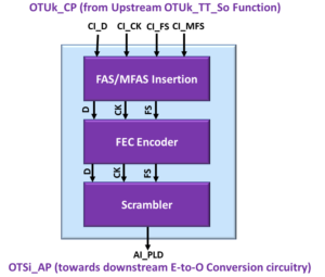
Figure 1 presents a simple illustration of the OTSiG/OTUk_A_So function.
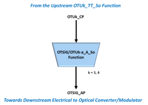
Figure 1, Simple Illustration of the OTSiG/OTUk_A_So function.
ITU-T G.798 defines two versions of this particular function. Additionally, there are other versions of this function that are not specified by ITU-T G.798. I list some popular versions of this function below in Table 1.
Table 1, List of Some Popular Versions for the OTSiG/OTUk_A_So function.
| Function Name | Description | Comments |
| OTSiG/OTUk-a_A_So | OTSiG to OTUk Adaptation Source Function with ITU-T G.709 Standard FEC. | Can be used for OTU3 and OTU4 applications ONLY. |
| OTSiG/OTUk-b_A_So | OTSiG to OTUk Adaptation Source Function with No FEC | Can only be used for OTU3 Applications.
Cannot be used for OTU4 applications. |
| OTSiG/OTUk-v_A_So | OTSiG to OTUk Adaptation Source Function with Vendor-Specific FEC | Can be used for OTU3 and OTU4 Applications.
Not specified by ITU-T G.798. |
Table 1 shows that the OTSiG/OTUk-a_A_So and the OTSiG/OTUk-v_A_So functions will compute and append some sort of FEC field to the back-end of each outbound OTUk frame.
However, this table also shows that the OTSiG/OTUk-b_A_So version does not generate the FEC field.
Consequently, ITU-T G.798 states that one can use the OTSiG/OTUk-a_A_So and OTSiG/OTUk-v_A_So functions for OTU3 and OTU4 applications. The standard also recommends that the user NOT use the OTSiG/OTUk-b_A_So function for OTU4 applications.
The OTU4 rate requires the use of Forward-Error-Correction.
What Version will we Discuss Throughout this Post?
Throughout this post, we will be discussing the OTSiG/OTUk-a_A_So version of this atomic function.
The OTSiG/OTUk-b_A_So and OTSiG/OTUk-v_A_So atomic functions do everything that the OTSiG/OTUk-a_A_So does, except that the -b version does NO FEC Encoding, and the -v version does FEC Encoding differently than what I describe here.
Stuck at Home? You Can Be an Expert on OTN Before You Return to Your Office!!! Click on the Banner Below to Learn More!!
Corporate Discounts Available!!!

So What All Does this Atomic Function Do?
The OTSiG/OTUk-a_A_So function will accept the OTUk data-stream, OTUk clock signal, frame-start signal, and multi-frame start signals via the CI_D, CI_CK, CI_FS, and CI_MFS inputs (of this function) respectively, and it will perform the following tasks.
- It will insert the FAS and MFAS fields into the outbound OTUk data stream (coincident with whenever the upstream OTUk_TT_So function asserts the CI_FS and CI_MFS inputs, respectively).
- This function will compute and append a FEC field to the back-end of each outbound OTUk frame.
- It will scramble this “combined” OTUk data stream (consisting of the FAS, MFAS, and FEC fields).
- Next, this function will demultiplex and combine this data stream into four parallel lanes of OTL3.4 traffic (for OTU3 applications) and OTL4.4 traffic (for OTU4 applications).
- This function will transmit these four lanes to external Electrical-to-Optical Conversion circuitry (which will convert our OTL3.4 or OTL4.4 traffic into the optical format).
I illustrate a Unidirectional Connection that shows where the OTSiG/OTUk-a_a_So function “fits in” within a system below in Figure 2.
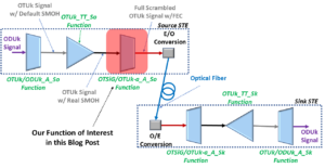
Figure 2, Illustration of an STE, transmitting an OTUk signal (over optical fiber) to another STE – the OTSiG/OTUk-a_A_So function is highlighted.
Figure 2 shows that the OTSiG/OTUk-a_A_So function will accept traffic from the upstream OTUk_TT_So function. The OTSiG/OTUk-a_A_So function will then perform additional processing on this data before it sends it over to optical circuitry for conversion and transport.
We will discuss this additional processing below.
Functional Description of this Atomic Function
Let’s take a closer look at this function now.
The OTSiG/OTUk-a_A_So functional blocks are different for OTU3 applications than for OTU4 applications. Therefore, we will first walk through the Functional Block Diagram for OTU3 applications.
Afterward, we will do the same for OTU4 applications.
Review of the OTSiG/OTU3-a_A_So Functional Block Diagram – OTU3 Applications
Figure 3 presents the Functional Block Diagram of the OTSiG/OTUk-a_A_So Atomic Function for OTU3 Applications.
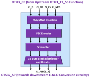
Figure 3, Illustration of the Functional Block Diagram of the OTSiG/OTU3-a_A_So Atomic Function (for OTU3 Applications).
Hence, Figure 3 shows that the OTU3-version of this function contains the following functional blocks.
- FAS/MFAS Insertion Block
- FEC Encoder Block
- Scrambler Block
- 16-Byte Block Distributor and Rotator Block
I will briefly discuss each of these functional blocks below.
The FAS/MFAS Insertion Block
The FAS/MFAS Insertion Block is the first block the OTU3 signal will pass through after entering this atomic function. I illustrate the OTSiG/OTU3-a_A_So function with the FAS/MFAS Insertion block highlighted below in Figure 4.
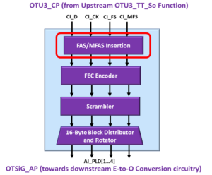
Figure 4, Illustration of the OTSiG/OTU3-a_A_So Functional Block Diagram with the FAS/MFAS Insertion Block highlighted.
The FAS/MFAS Insertion block will insert the FAS and MFAS fields into the outbound OTU3 data stream each time the upstream OTUk_TT_So function asserts the CI_FS input pin.
Likewise, the FAS/MFAS Insertion block will initialize the MFAS byte-field to 0x00 within the outbound OTU3 data stream each time the upstream OTUk_TT_So function asserts the CI_MFS input pin.
The FAS/MFAS Insertion block will proceed to increment the contents of the MFAS field within each OTU3 frame it generates.
The FEC Encoder Block
Once the OTU3 signal leaves the FAS/MFAS Insertion block, it will pass through the FEC Encoder block. I show an illustration of the OTSiG/OTU3-a_A_So Functional Block Diagram, with the FEC Encoder Block Highlighted below in Figure 5.
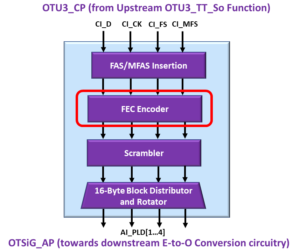
Figure 5, Illustration of the OTSiG/OTU3-a_A_So Functional Block Diagram with the FEC Encoder block highlighted.
The FEC Encoder block will compute the FEC field and append this field to the back-end of each outbound OTU3 frame.
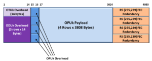
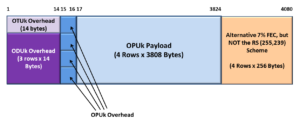
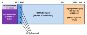
ITU-T G.709 recommends that (for a Fully-Compliant OTUk Frame), one uses the Reed Solomon RS(255,239) Code for its Forward-Error-Correction scheme.
The standard also recommends that the System Designer use Symbol-Interleaving and that the user place the resulting FEC code into a 4-row x 256-byte column field at the back-end of each outbound OTUk frame.
I show the location (that the FEC Encoder block should insert the FEC Code) within the OTUk frame below in Figure 6.
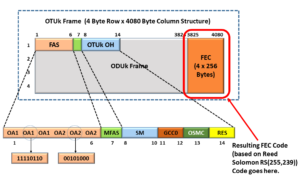
Figure 6, Illustration of the OTUk Frame, with the Location of the FEC-field highlighted
I discuss this Forward-Error-Correction scheme in much greater detail in another post.
Once this OTU3 data stream leaves the FEC Encoder block, it will proceed to the Scrambler block for further processing.
The Scrambler Block
I illustrate the OTSiG/OTU3-a_A_So Functional Block Diagram with the Scrambler Block highlighted below in Figure 7.
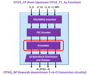
Figure 7, Illustration of the OTSiG/OTU3-a_A_So Functional Block Diagram with the Scrambler Block highlighted.
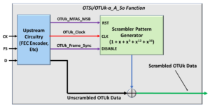
ITU-T G.709 requires that we scramble OTUk data before we transmit it over optical fiber.
The standard requires that we do this to ensure that this OTUk signal has sufficient bit-timing content for Clock and Data Recovery PLLs (Phase-Locked Loops) within the Sink STE (at the remote end).
ITU-T G.709 also states that the Scrambler must operate as a frame synchronous scrambler of sequence length 65,535 (e.g., 216-1), running at the OTUk rate.
Finally, ITU-T G.709 states that the Scrambler must use the generating polynomial of 1 + x + x3 + x12 + x16.
I show a simple diagram of how the user can implement the Scrambler within their OTSiG/OTUk-a_A_So function design below in Figure 8.
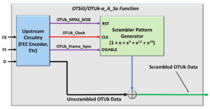
Figure 8, Illustration of the High-Level Block Diagram for the Frame-Synchronous Scrambler
Has Inflation got You Down? Our Price Discounts Can Help You Fight Inflation and Help You Become an Expert on OTN!! Click on the Banner Below to Learn More!!!
Discounts Available for a Short Time!!!
16-Byte Block Distributor and Rotator Block
Once the OTU3 signal leaves the Scrambler block, it will pass through the 16-Byte Block Distributor and Rotator Block. I illustrate the OTSiG/OTU3-a_A_So Functional Block Diagram with the 16-Byte Block Distributor and Rotator Block highlighted below in Figure 9.
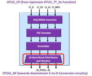
Figure 9, Illustration of the OTSiG/OTU3-a_A_So Functional Block Diagram with the 16-Byte Block Distributor and Rotator Block highlighted.
The 16-Byte Block Distributor and Rotator block will convert a composite OTU3 signal (that is of the form of a single serial data stream) into the OTL3.4 format (over four lanes) that we describe in the OTL3.4 post.
In this case, the OTSiG/OTU3-a_A_So function has four outputs (one output for each of the four OTL3.4 lanes), which we labeled AI_PLD[1] through AI_PLD[4] in Figure 9.
The user is expected to connect these four output signals to optical circuitry (that will convert this electrical data into the optical format).
We have briefly covered the OTSiG/OTUk-a_A_So function block for OTU3 applications. Let’s move on and discuss this atomic function for OTU4 applications.
Review of the OTSiG/OTU4-a_A_So Functional Block Diagram – OTU4 Applications
I present the Functional Block Diagram of the OTSiG/OTUk-a_A_So Atomic Function for OTU4 Applications below in Figure 10.
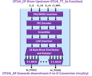
Figure 10, Illustration of the Functional Block Diagram of the OTSiG/OTU4-a_A_So Atomic Function (for OTU4 Applications)
Hence, Figure 4 shows that the OTU4 version of this function contains the following functional blocks.
- FAS/MFAS Insertion Block
- FEC Encoder Block
- Scrambler Block
- LLM (Logical Lane Marker) Insertion Block
- 16 Byte Block Distributor and Rotator Block
I will discuss some of these Functional blocks below. Please note that some of these blocks are identical to what I’ve presented for OTU3 applications. I will note that whenever I come to those functional blocks.
The FAS/MFAS Insertion Block
Please see the description for the FAS/MFAS Insertion Block above for OTU3 applications.
The FEC Encoder Block
Please see the description for the FEC Encoder Block above for OTU3 applications.
The Scrambler Block
Please see the description for the Scrambler Block above for OTU3 applications.
The LLM (Logical Lane Marker) Insertion Block
Once the OTU4 signal passes through and leaves the Scrambler block, it will pass through the LLM Insertion block.
I show an illustration of the OTSiG/OTU4-a_A_So Functional Block Diagram with the LLM Insertion Block Highlighted below in Figure 11.
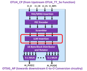
Figure 11, Illustration of the OTSiG/OTU4-a_A_So Functional Block Diagram, with the LLM Insertion Block highlighted.
Two things happen at the LLM Insertion Block.
- We start the process of demultiplexing the OTU4 data stream into 20 logical lanes, and
- We identify these Logical Lanes by inserting the appropriate LLM value into each of these 20 logical lanes (or data streams).
If you recall from the OTL4.4 blog post, whenever we encode an OTU4 signal into the OTL4.4 format, we will borrow the 3rd OA2 byte-field (within the FAS field) and use it as the Logical Lane Marker.
I show an illustration of the OTUk Framing Format, with this particular FAS byte highlighted below in Figure 12.
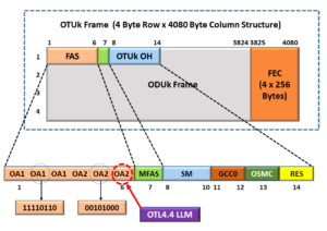
Figure 12, Illustration of the OTUk Framing Format, with the 3rd OA2 Byte-field (that we use for the LLM – for OTL4.4 applications) highlighted.
The purpose of the LLM Insertion Block is to insert a value into this “borrowed FAS-byte field” that ranges in value from 0 to 239. This value (that we insert into this LLM field) functions as the Logical Lane ID for each of the 20 Logical Lanes.
Please see the OTL4.4 Blog Post for more information on the assignment of these Logical Lane IDs.
The 16-Byte Block Distributor and Rotator Block
Once the OTU4 signal exits the LLM Insertion Block, it will pass through the 16-Byte Block Distributor and Rotator Block.
I illustrate the OTSiG/OTU4-a_A_So functional block diagram with the 16-Byte Block Distributor and Rotator block highlighted below in Figure 13.
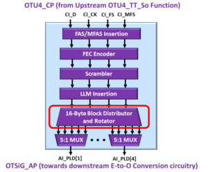
Figure 13, Illustration of the OTSiG/OTU4-a_A_So Functional Block Diagram with the 16-Byte Block Distributor and Rotator Block highlighted.
The 16-Byte Block Distributor and Rotator Block will work with the LLM Insertion Block to demultiplex a serial OTU4 data stream into 20 logical lane signals.
Please see the OTL4.4 post for most information about the 16-Byte Block Distributor and Rotator block.
This block will then route these 20 logical lanes (with their LLM ID included) downstream towards their 5:1 Bit-Wise Multiplexers.
The 5:1 Bit-Wise Multiplexers
After the LLM Insertion and 16-Byte Distributor and Rotator blocks have demultiplexed the single OTU4 signal into 20 Logical Lane signals, these blocks will send these 20 Logical Lane signals to a set of four 5:1 Bit-Wise Multiplexers.
I illustrate the OTSiG/OTU4-a_A_So Functional Block Diagram with a set of four 5:1 Bit-Wise Multiplexers highlighted below in Figure 14.
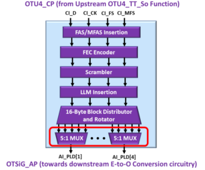
Figure 14, Illustration of the OTSiG/OTU4-a_A_So Functional Block Diagram, with a set of four 5:1 Bit-Wise Multiplexers highlighted
The OTSiG/OTU4-a_A_So function will route each of the 20 Logical Lane signals to one of four 5:1 Bit-Wise Multiplexers. Each of these 5:1 Bit-Wise Multiplexers will accept 5 Logical Lane signals. These Bit-Wise Multiplexers will then bit-wise multiplex these five signals into a single electrical lane.
Therefore, since we are applying 20 Logical Lane signals to these four 5:1 Bit-Wise Multiplexers, we will combine these 20 Logical Lane signals into four electrical lane signals. These bit-wise multiplexed 4-lane signals are our OTL4.4 signal that we can route to the nearby optical circuitry.
The OTSiG/OTU4-a_A_So function will output these four electrical signals to optical circuitry via the AI_PLD[1] through AI_PLD[4] output signals.
Function Defects
This function does not declare any defect conditions.
Function Consequent Equations
This function does not have any Consequent Action (or Equations).
Pin Description of the OTSiG/OTUk-a_A_So Function
Table 2 presents a list and description of each of the Input and Output pins of the OTSiG/OTUk-a_A_So Function.
Table 2, Pin Description of the OTSiG/OTUk-a_A_So Atomic Function
| Signal Name | Type | Description |
| OTUk_CP Interface | | |
| CI_D | Input | OTUk Characteristic Information - OTUk Data Input:
The OTSiG/OTUk-a_A_So function will accept this OTU3 or OTU4 data-stream from the upstream OTUk_TT_So function. The OTSiG/OTUk-a_A_So atomic function will then convert this single OTU3 or OTU4 data-stream into the OTL3.4 or OTL4.4 format, respectively.
This OTUk data-stream will NOT include the FAS, MFAS or FEC fields.
This particular function will compute and append the FEC field to the back-end of each outbound OTU3/4 frame. This function will also use the CI_FS and CI_MFS signal to insert the FAS and MFAS fields into this single OTU3/4 data-stream, all prior to demultiplexing this OTU3/4 data-stream into 4 lanes of traffic. |
| CI_CK | Input | OTUk Characteristic Information - Clock Input:
The OTSiG/OTUk-a_A_So function will sample all data and signals (at the OTUk_CP Interface) upon one of the edges of this input clock signal. This statement applies to the CI_D, CI_FS and CI_MFS input signals.
This clock signal will also function as the timing source for this function as well. |
| CI_FS | Input | OTUk Characteristic Information - Frame Start Output:
The upstream OTUk_TT_So function will drive this output pin HIGH whenever that function outputs the very first bit (or byte) of a new OTUk frame, via the CI_D input.
The OTUk_TT_So function should only pulse this output pin HIGH once for each incoming OTUk frame.
The OTSiG/OTUk-a_A_So function will use this input signal to determine where it should denote the boundary of each OTUk frame and insert the FAS, MFAS and FEC fields into the serial OTUk data-stream, prior to it demultiplexing this data-stream into 4 electrical lanes of traffic. |
| CI_MFS | Input | OTUk Characteristic Information - Multi-Frame Start Input:
The upstream OTUk_TT_So function will drive this output pin HIGH whenever it applies the very first bit (or byte) of a new OTUk multiframe to the CI_D input.
The upstream OTUk_TT_So function will drive this output pin HIGH once for each OTUk multi-frame.
The OTSiG/OTUk-a_A_So function will use this input to determine, at which OTUk frame, it should initialize the MFAS byte-field to 0x00 (to denote the start of a new Multi-Frame). |
| OTSi_AP Interface | | |
| A_PLD[1] | Output | OTL3.4 or OTL4.4 Electrical Output - Lane 1:
After the OTSiG/OTUk-a_A_So function computes and inserts the FEC and also includes the FAS and MFAS fields, it will demultiplex that composite OTU3/OTU4 data-stream into either the OTL3.4 or OTL4.4 format.
This particular output is Lane 1 for this 4-Lane Electrical Interface. |
| A_PLD[2] | Output | OTL3.4 or OTL4.4 Electrical Output - Lane 2:
Please see the description for AI_PLD[1]. |
| A_PLD[3] | Output | OTL3.4 or OTL4.4 Electrical Output - Lane 3:
Please see the description of AI_PLD[3]. |
| A_PLD[4] | Output | OTL3.4 or OTL4.4 Electrical Output - Lane 4:
Please see the description of AI_PLD[1]. |
Clueless about OTN? We Can Help!! Click on the Banner Below for More Information!!!
Discounts Available for a Short Time!!
Click on the Image below for More Blog Posts on Optical Transport Networks.

OTN Related Topics within this Blog General Topics Consequent Equations - What are they and How can you use them? ...