OTN – Lesson 9 – Video 11 – OTU Layer Defect Handling Requirements and Scenarios

In this video, we presume that some OTUk-Layer circuitry is declaring a certain defect condition. We then determine how OTU (and in some cases) ODU-layer circuitry is expected to respond.

OTN – Lesson 9 – Video 11 – OTU Layer Defect Scenarios

This blog post presents a video that discusses the various defects that OTN equipment can declare at the OTU Layer.  Additionally, this video will describe how OTU Layer circuitry should respond to and handle these defect conditions.  

This video will state whether OTU Layer circuitry should:

  • Transmit the SM-BDI Indicator upstream, or 
  • Transmit the ODU-AIS Maintenance Signal downstream, 
  • Increment Certain Performance Monitoring parameters, or
  • Halt Incrementing Certain Performance Monitoring parameters.

In response to each type of defect that OTU Layer circuitry can declare.

This video covers both Single-Lane (e.g., OTSi/OTUk_A_Sk) and Multi-Lane (e.g., OTSiG/OTUk_A_Sk) applications. 

Continue reading “OTN – Lesson 9 – Video 11 – OTU Layer Defect Handling Requirements and Scenarios”

OTN – Lesson 9 – Video 6 – OTU Layer Sink Direction Circuitry – OTSi/OTUk_A_Sk Function

This post presents the 6th of the 11 Videos that covers training on Performance Monitoring at the OTU Layer. This post focuses on the Sink Direction OTU-Layer Atomic Functions.

OTN – Lesson 9 – Video 6 – OTU Layer Sink Direction Circuitry/Functionality – Part 4

This blog post contains a video that focuses on the OTSi/OTUk_A_Sk Atomic Function.  

The OTSi/OTUk_A_Sk Function has many of the same features/functionality as the OTSiG/OTUk_A_Sk Function.  

However, the OTSi/OTUk_A_Sk function supports the transport/reception of an OTU signal over a Single-Lane Connection (instead of 4 electrical lanes – such as the OTL3.4 or OTL4.4 Interface). Hence, this Atomic Function applies to OTU1 and OTU2 applications.  

The main difference between the OTSi/OTUk_A_Sk function and the OTSiG/OTUk_A_Sk function is that the OTSi/OTUk_A_Sk function will detect and declare the OTUk-AIS defect.  

Continue reading “OTN – Lesson 9 – Video 6 – OTU Layer Sink Direction Circuitry – OTSi/OTUk_A_Sk Function”

Declaring/Clearing dAIS Defect (OTUk)

This post describes how an OTN STE (Section Terminating Equipment) should declare and clear the dAIS Defect Condition (OTUk-AIS).

How Should an OTN STE Declare and Clear the dAIS Defect Condition (OTUk-AIS)?

In another post, we describe the OTUk-AIS Maintenance Signal

Further, in that post, I stated that ITU-T G.709 does not require that an OTN STE be able to generate and transmit the OTUk-AIS Maintenance Signal.  

However, I also stated that ITU-T G.709 DOES require that an OTN STE be capable of receiving and processing the OTUk-AIS Maintenance signal, such that it can declare and clear the OTUk-AIS defect condition.  

What about this Post?  

This post will discuss how an STE should declare and clear the dAIS (OTUk-AIS) defect.

NOTE:  Please do not confuse this particular dAIS Defect (in response to the detection of the OTUk-AIS Maintenance signal) with the other AIS Defect (in response to receipt of the ODUk-AIS Maintenance Signal). 

Although their names are similar, they are two very different maintenance signals and defects.

The OTUk-AIS Maintenance Signal Post states that the OTUk-AIS Maintenance Signal is an Unframed PN-11 Pattern. More specifically, ITU-T G.709 defines this PN-11 sequence by the generating polynomial:  1 + x9 + x11.

How to Detect the PN-11 Pattern?

If we want to detect, declare, and clear the dAIS condition, then we need to have some ability to detect this unframed PN-11 pattern.

Fortunately, the ITU-T Standard Committee did much of the work for us and defined such a circuit within ITU-T G.798.

I show this Inverse PN-11 Circuit below in Figure 1.

Inverse PN-11 Detector - for dAIS (OTUk-AIS) Detection

Figure 1, Illustration of the Inverse PN-11 Circuit

How Does this Inverse PN-11 Circuit Work?

This Inverse PN-11 Circuit makes up a big part of our dAIS Detection Circuit (that we also mention in the post on the OTSi/OTUk_A_Sk atomic function).

The user should apply the Recovered OTUk Data and Clock Signal at the IN and Clock inputs of our Inverse PN-11 Circuit, respectively.

If our OTUk data-stream is carrying the OTUk-AIS Maintenance signal (e.g., an Unframed PN-11 signal) and if we are applying this data to the IN input (of our circuit), then our Inverse PN-11 circuit will generate an All-Zeros Pattern at the Node, that I’ve labeled OUT.

I show our Inverse PN-11 Circuit, again, below in Figure 2. However, in this figure, I also highlight these two reference points.

OTUk-AIS is applied to Inverse PN-11 Detector

Figure 2, Illustration of the Inverse PN-11 Circuit – with the Locations of the OTUk-AIS Maintenance Signal and the Resulting All-Zeros Pattern Highlighted.  

Before we get too excited, we need to recognize that two conditions will cause our Inverse PN-11 circuit to generate an All-Zeros Pattern at the OUT node.

  1. Our Inverse PN-11 Circuit will generate the All-Zeros pattern at the OUT Node whenever the OTUk-AIS Maintenance Signal is present at the IN input (to this circuit), and
  2. Our Inverse PN-11 Circuit will also generate the AIl-Zeros pattern (at the OUT Node) whenever someone applies an All-Zeros Pattern at the IN Input.

OTUk-AIS Maintenance Signal or All-Zeros Pattern Signal at the IN input?

Hence, whenever we use the Inverse PN-11 Circuit to check for the OTUk-AIS Maintenance signal, we (of course) need to check the OUT Node (or our Inverse PN-11 Circuit).

However, we also need to check and ensure that we are NOT receiving an All-Zeros pattern at the IN input.

If we are TRULY receiving the OTUk-AIS Maintenance Signal, we will see an All-Zeros pattern at the OUT Node, while the signal at the IN input is NOT an All-Zeros pattern.

I summarize how the Inverse PN-11 Detector circuit works for various signals (at the IN input) below in Table 1.

Table 1, A Truth Table presenting How the Inverse PN-11 Detector Circuit responds to Various Signals (at the IN input)

IN InputOUT NodeComments
All-Zeros SignalAll-Zeros SignalAn All-Zeros pattern at the IN Input results in an All-Zeros pattern at the OUT Node.

No OTUk-AIS.
Ordinary OTUk TrafficNon All-Zeros Pattern SignalNormal Traffic Situation
OTUk-AIS Maintenance SignalAll-Zeros SignalThe Presence of an All-Zeros Signal at the OUT Node, and the Non All-Zeros pattern at the IN input indicates OTUk-AIS.

Stuck at Home? You Can Become an Expert in OTN Before You Return to Your Office. Click on the Banner Below to Learn More!!!

Corporate Discounts Available for a Short Time!!

Criteria for Declaring the dAIS Defect?

OK, we now have a basic understanding of how the Inverse PN-11 Detector circuit works. We also know what signals to look for to determine if the Inverse PN-11 Circuit detects the OTUk-AIS Maintenance signal

Let’s now move on to the full criteria for declaring the dAIS defect.

When checking for dAIS, ITU-T G.798 recommends that we continuously monitor both of the signals at the  IN input signal and the OUT Node of our Inverse PN-11 Circuit.

ITU-T G.798 goes on to (effectively) state that we should continuously check these signals over a rolling 8192 bit-interval (or sliding window, if you will).

If our Inverse PN-11 circuit detects a set of three (3) consecutive strings each of 8192-bit periods (in length), such that BOTH of the following conditions are TRUE for each of these three 8192 bit-periods, then we MUST declare the dAIS defect condition.

  • The number of 1s bits at the OUT Node is less than 256; AND
  • the number of 1s bits at the IN Input is 256 or more.

I show an illustration of the dAIS Defect Declaration Criteria below in Figure 3.

dAIS Defect Declaration Criteria

Figure 3, Illustration of the dAIS (OTUk-AIS) Defect Declaration Criteria

Criteria for Clearing the dAIS Defect Condition

On the other hand, while we are declaring the dAIS defect, if our Inverse PN-11 circuit detects a set of three (3) consecutive strings, each of 8192-bit periods (in length) such that EITHER of the following conditions is TRUE for each of these three 8192 bit periods, then we MUST clear the dAIS defect condition.

  • If the number of 1s bits at the OUT Node is 256 or more, OR
  • If the number of 1s bits at the IN input is less than 256 in three consecutive 8192-bit intervals.

I show an illustration of the dAIS Defect Clearance Criteria below in Figure 4.

OTUk-AIS Defect Clearance Criteria

Figure 4, Illustration of the dAIS (OTUk-AIS) Defect Clearance Criteria

What Entities or Atomic Functions declare and clear the dAIS (OTUk-AIS) defect condition?

The OTSi/OTUk_A_Sk function is the only atomic function that contains an Inverse PN-11 Detector circuit. Hence, it is the one atomic function that will declare or clear the OTUk-dAIS Defect condition.  

NOTE:  For Multi-Lane Applications, the OTSiG/OTUk_A_Sk function does not contain an Inverse PN-11 Detector circuit nor declare or clear the dAIS Defect condition.

If for some reason, an OTL3.4 or OTL4.4 signal were carrying the OTUk-AIS Maintenance Signal (which, again, is an Unframed PN-11 Pattern), then the OTSiG/OTUk_A_Sk function (that is receiving this signal) would instead, continuously declare the dLOFLANE defect condition(*) within each of the 4 or 20 Logical Lanes. 

This atomic function would also declare the dLOL defect(*) as well.

NOTE:  (*) – Indicates that you need to be a member of THE BEST DARN OTN TRAINING PRESENTATION…PERIOD!! to access these links.  

Clueless about OTN? We Can Help!! Click on the Banner Below to Learn More!!

Discounts Available for a Short Time!!

Click on the Image below to See More OTN-Related Posts

OTN Related Blog

OTN Related Topics within this Blog

OTN Related Topics within this Blog General Topics Consequent Equations - What are they and How can you use them? ...

What is the OTSi/OTUk_A_Sk Function?

This blog post briefly describes the OTSi/OTUk_A_Sk (OTSi to OTUk Adaptation Sink) Atomic Function. This post also describes how this atomic function declares and clears the dLOF, dLOM, and dAIS defects.


What is the OTSi/OTUk_A_Sk Atomic Function?

The expression:  OTSi/OTUk_A_Sk is an abbreviation for the term:  Optical Tributary Signal to OTUk Adaptation Sink Function.

This blog post will briefly describe the OTSi/OTUk_A_Sk set of atomic functions.

We discuss the OTSi/OTUk_A_Sk Atomic Function in detail in Lesson 9, within THE BEST DARN OTN TRAINING PRESENTATION…PERIOD!!!

Changes in Terminology

Before we proceed on with this post, we need to cover some recent changes in terminology.  Before the June 2016 Version of ITU-T G.709, the standard documents referred to this particular atomic function as the OCh/OTUk_A_Sk function.

However, the standards committee has recently decided to change the wording from using the term OCh (for Optical Channel) to OTSi (for Optical Tributary Signal).

For completeness, I will tell you that ITU-T G.959.1 defines the term OTSi as:

“Optical signal that is placed within a network media channel for transport across the optical network.  This may consist of a single modulated optical carrier or a group of modulated optical carriers or subcarriers”.

Hence, to “speak the same language” as the standard committee, we will call this atomic function the OTSi/OTUk_A_Sk atomic function.

Likewise, in another post, we will now call (what we used to call the OCh/OTUk_A_So function) the OTSi/OTUk_A_So function.

I have created another post that provides documentation of the relationships between some old (now obsolete) terms and the new (and approved) ones that our standard committee is currently using.

The OTSi/OTUk_A_Sk Function

The OTSi/OTUk_A_Sk function is any circuit that takes an OTSi electrical signal and converts this data back into the OTUk signal.

More specifically, the System-Designer will apply an OTSi signal (which will be a fully-framed and scrambled OTUk electrical signal that often includes Forward-Error-Correction) to the OTSi_AP input interface.

This function will convert this signal into OTUk data, clock, frame start, and multi-frame start signals.

This function will also decode the Forward-Error-Correction field (if available) and output these signals to downstream circuitry (such as the OTUk_TT_Sk function).

ITU-T G.798 states that the system designer can use this function for all OTUk rates (e.g., from OTU1 through OTU4).

However, in most cases, we will typically use the OTSi/OTUk_A_Sk function for OTU1 and OTU2 applications.  We will usually use the OTSiG/OTUk_A_Sk atomic function for OTU3 and OTU4 applications.

We discuss the OTSiG/OTUk_A_Sk atomic function in another post.

Figure 1 presents a simple illustration of the OTSi/OTUk_A_Sk function.

OTSi/OTUk-a_A_So Simple Function Drawing

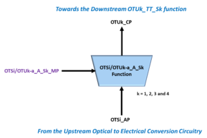
Figure 1, Simple Illustration of the OTSi/OTUk_A_Sk function

ITU-T G.798 defines three versions of this particular function.  I have listed these versions below in Table 1.

Table 1, List of the ITU-T G.798 -specified Versions for the OTSi/OTUk_A_Sk functions

Function NameDescriptionComments
OTSi/OTUk-a_A_SkOTSi to OTUk Adaptation Sink Function with ITU-T G.709 Standard FECCan be used for OTU1 through OTU4 applications.
OTSi/OTUk-b_A_SkOTSi to OTUk Adaptation Sink Function with No FECCannot be used for OTU4 applications
OTSi/OTUk-v_A_SkOTSi to OTUk Adaptation Sink Function with Vendor-Specific FECCan be used for OTU1 through OTU4 applications.

Table 1 shows that the OTSi/OTUk-a_A_Sk and the OTSi/OTUk-v_A_Sk functions will compute and decode some sort of FEC field within the backend of each incoming OTUk frame.

However, this table also shows that the OTSi/OTUk-b_A_Sk version does not support FEC decoding.

Therefore, ITU-T G.798 states that one can use the OTSi/OTUk-a_A_Sk and OTSi/OTUk-v_A_Sk functions for OTU1 through OTU4 applications.  Further, the standard recommends that the user NOT use the OTSi/OTUk-b_A_Sk function for OTU4 applications.

Network Terminals operating at the OTU4 rate are required to use Forward-Error-Correction.

Clueless about OTN? We Can Help!!! Click on the Banner Below to Learn More!!!

Corporate Discounts Available!!!

What Version (of the OTSi/OTUk_A_Sk function) will we Discuss Throughout this Post?

Throughout this post, we will be discussing the OTSi/OTUk-a_A_Sk version of this atomic function.

The OTSi/OTUk-b_A_Sk and OTSi/OTUk-v_A_Sk atomic functions do everything that the OTSi/OTUk-a_A_So does, except that the -b version does NO FEC Decoding and the -v version does FEC Decoding differently than what I describe here.

So What All Does this Atomic Function Do?

The OTSi/OTUk-a_A_Sk function will accept an OTSi data stream from the upstream Optical-to-Electrical Conversion circuitry.  This function will perform the following tasks on this incoming data stream.

  • Descrambling – It will descramble this incoming data stream.
  • FEC Decoding – The function will decode the FEC field (within the backend of each incoming OTUk frame) and detect and correct most symbol errors within this data stream.
  • Extract the Frame-Start and Multi-Frame Start signals from this incoming data stream.
  • Detect and Flag the following service-affecting defect conditions
  • Assert the CI_SSF (Server Signal Fail Indicator) output signal (towards the downstream OTUk_TT_Sk function) anytime it declares any service-affecting defect conditions.
  • Output the remaining OTUk data stream, the OTUk clock signal, the Frame-Start, and Multi-Frame Start signals to downstream circuitry (e.g., typically the OTUk_TT_Sk atomic function).

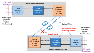
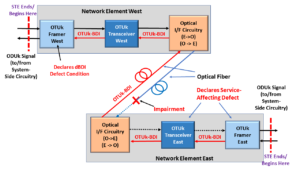
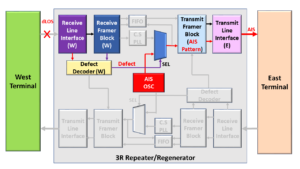
Figure 2 illustrates a Unidirectional Connection where the OTSi/OTUk-a_A_Sk function “fits in” a system.

OTSi/OTUk-a_A_Sk Function Highlighted in Unidirectional OTUk End-to-End Connection

Figure 2, Illustration of an STE, transmitting an OTUk signal (over optical fiber) to another STE – the OTSi/OTUk-a_A_Sk function is highlighted. 

Functional Description of this Atomic Function

Let’s now take a closer look at this function.

Figure 3 presents the Functional Block Diagram of the OTSi/OTUk-a_A_Sk Atomic Function.

OTSi/OTUk-a_A_Sk Functional Block Diagram

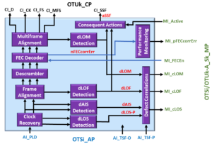
Figure 3, Illustration of the Functional Block Diagram of the OTSi/OTUk-a_A_Sk Atomic Function

Therefore, Figure 3 shows that this function contains the following functional blocks

I will briefly discuss each of these functional blocks below.

The Clock Recovery and dLOS (Loss of Signal Defect) Detection Blocks

The Clock Recovery block is responsible for recovering the clock signal and data content within the incoming OTSi signal via the AI_PLD input pin.

To that end, I illustrate the OTSi/OTUk-a_A_Sk Functional Block Diagram with the Clock Recovery and dLOS Detection Blocks highlighted below in Figure 4.

OTSi/OTUk-a_A_Sk Functional Block Diagram - dLOS Detection Block Highlighted

Figure 4, Illustration of the OTSi/OTUk-a_A_Sk Functional Block Diagram, with the Clock Recovery and dLOS Detection Blocks highlighted. 

Since the OTSi/OTUk-a_A_So atomic function (within the remote STE) should have scrambled this data stream, there should always be good timing content (or transitions) within the incoming OTSi signal so that this Clock Recovery block can acquire and extract out both a recovered clock signal and data-stream.

Suppose the Clock Recovery and dLOS Detection blocks determine a lengthy absence in signal transitions (within the incoming OTSi data-stream).  It will declare the dLOS-P (Loss of Signal-Path) defect condition in that case.

Please check out the dLOS blog post for more information about the dLOS-P defect condition.

The OTSi/OTUk-a_A_Sk function will route this recovered clock and data signal to the dAIS Detector and Frame Alignment blocks for further processing.

Stuck at Home? You Can Be an Expert on OTN Before You Return to Your Office!!! Click on the Banner Below to Learn More!!!

Discounts Available for a Short Time!!!

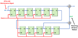
The dAIS (Alarm Indication State Defect) Detector Block

As the newly recovered clock and data signal travel to the Frame Alignment block, the dAIS Detector block will also parse through this data stream to see if it should declare or clear the dAIS (Alarm Indication Signal Defect) condition or not.

To make things more convenient, I present an illustration of the OTSi/OTUk-a_A_Sk Functional Block Diagram, with the AIS Detector block highlighted below in Figure 5.

OTSi/OTUk-a_A_Sk Functional Block Diagram with dAIS Detection Circuitry Highlighted

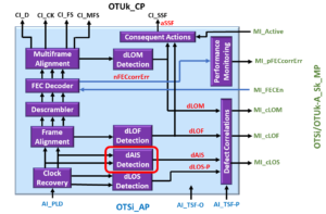
Figure 5, Illustration of the OTSi/OTUk-a_A_Sk Functional Block Diagram, with the AIS Detector block highlighted. 

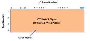
In this case, the dAIS Detector block will check to see if the incoming data stream matches an OTUk-AIS maintenance signal.

ITU-T G.709 further states that the OTUk-AIS maintenance signal is an unframed PN-11 repeating pattern.

The standard defines the PN-11 sequence by the generating polynomial of 1 + x9 + x11.

Please see the blog post on the OTUk-AIS Maintenance signal for more information about this type of signal.

Additionally, please see the dAIS post for more information on how the AIS Detection circuit declares and clears the dAIS defect condition.

The Frame Alignment and dLOF (Loss of Frame Defect) Detection Blocks

As long as the dAIS Detector block is NOT declaring the dAIS defect condition, then the Frame Alignment block will process the incoming recovered block and data stream.

To make things more convenient for you, I present an illustration of the OTSi/OTUk-a_A_Sk Functional Block Diagram.  This block diagram highlights the Frame Alignment and dLOF Detection below in Figure 6.

OTSi/OTUk-a_A_Sk Functional Block Diagram - dLOF Detection Circuitry

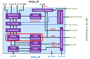
Figure 6, Illustration of the OTSi/OTUk-a_A_Sk Functional Block Diagram with the Frame Alignment and dLOF Detection circuitry highlighted.

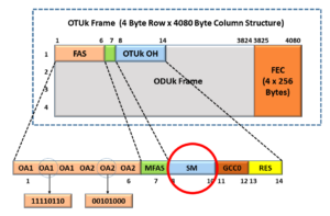
The incoming recovered data stream should be a full, scrambled OTUk frame.  However, the FAS field (e.g., the three OA1 and OA2 byte fields) should NOT be scrambled.

The Frame Alignment block will parse through the FAS fields within the incoming OTUk data stream.  This block and the dLOF (Loss of Frame) Detection Block will declare and clear the dLOF defect as appropriate.

Please see the blog post on the dLOF defect for more information about how the Frame Alignment and dLOF Detection blocks declare and clear the dLOF defect condition.

Descrambler Block

In the OTSi/OTUk-a_A_So  blog post, we mentioned that the OTSi/OTUk-a_A_So function would scramble the content of each OTUk frame.

That function will scramble all bytes (within each OTUk frame) except for the FAS fields.  This function will even scramble the MFAS field as well.

The purpose of the Descrambler block is to restore the content of each OTUk frame to its original state before being scrambled at the remote STE.

To that end, I illustrate the OTSi/OTUk-a_A_Sk Functional Block Diagram with the Descrambler block highlighted below in Figure 7.

OTSi/OTUk-a_A_Sk Functional Block Diagram with Descrambler Circuit Highlighted

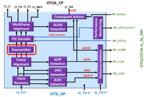
Figure 7, Illustration of the OTSi/OTUk-a_A_Sk Functional Block Diagram, with the Descrambler block highlighted.  

In the OTSi/OTUk-a_A_So function, we scrambled the contents of each OTUk frame, using the polynomial generating equation of 1 + x + x3 + x12 + x16.

Therefore, the Descrambler block (within this function) will descramble the incoming OTUk data-stream (again) using the polynomial generating equation of 1 + x + x3 + x12 + x16.

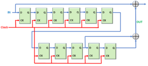
I show a simple diagram of how one can implement the Descrambler within their OTSi/OTUk-a_A_Sk function design below in Figure 8.

OTUk Descrambler Block within the OTSi/OTUk-a_A_Sk Function

Figure 8, High-Level Block Diagram of the Frame Synchronous Descrambler

I discuss the Descrambler function and requirements in greater detail in another post.

Next, the OTUk signal will proceed to the FEC Decoder block for further processing.

FEC (Forward-Error-Correction) Decoder Block

The OTSi/OTUk-a_A_So function (at the remote STE) is responsible for performing FEC (Forward Error Correction) Encoding.

This means that this function computed a FEC Code and inserted that code into a 4-row x 128-byte column field at the backend of each OTUk frame, as shown below in Figure 9.

OTUk Frame with FEC Field highlighted

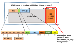
Figure 9, Illustration of the OTUk Frame Format with the FEC Field Highlighted

The purpose of the FEC Decoder (within the OTSi/OTUk-a_A_Sk function) is to parse through the incoming OTUk data stream and (by using the contents of the FEC-field) detect and correct most symbols errors within this data stream.

The FEC Decoder block will tally any occurrences of Symbol errors (within the incoming OTUk data stream).  It will report this information to System Management via the MI_pFECcorrErr output (via the OTSi/OTUk-a_A_Sk_MP Interface).

I discuss this Forward-Error-Correction scheme in much greater detail in another post.

Multi-Frame Alignment and dLOM (Loss of Multi-Frame Defect) Detection Blocks

Once the incoming OTUk data stream passes through the FEC Decoder block, the OTSi/OTUk-a_A_Sk function will route this signal to the Multi-Frame Alignment and dLOM Detection blocks.

The Multi-Frame Alignment block will parse through and check the contents of the MFAS field within the incoming OTUk data stream.  The Multi-Frame Alignment block will check the contents of this data stream to see if it (and the dLOM Detection Block) should declare or clear the dLOM defect condition.

Please see the blog post on the dLOM Defect for more information on how the Multi-Frame Alignment block will declare and clear the dLOM defect condition.

Removal of the FAS, MFAS, and FEC Fields from the incoming OTUk Data-stream

The Frame-Alignment block will drive the CI_FS (Frame-Start) output of the OTUk_CP Interface, HIGH for one CI_CK (Clock Signal) period, each time it detects the FAS field within its incoming OTUk data-stream.

Likewise, the Multi-Frame Alignment block will drive the CI_MFS (Multi-Frame Start) output of the OTUk_CP Interface, HIGH, for one CI_CK (Clock Signal) period each time it receives an MFAS byte with the value of 0x00.

The Frame-Alignment and Multi-Frame Alignment block will also remove the FAS and MFAS fields from the OTUk data stream (before it outputs this data stream via the CI_D output of the OTUk_CP Interface).

From this point on, the CI_FS and CI_MFS signals will now carry the framing and multi-framing alignment information downstream toward the OTUk_TT_Sk atomic function.

The FEC Decoder block will also remove the contents of the FEC field from the OTUk data stream before it outputs this data via the CI_D output pin.

Consequent Actions Block

In most cases, the Consequent Actions block will consist of digital logic circuitry that will assert the CI_SSF (Server Signal Fail) Output (of the OTUk_CP Interface) anytime the OTSi/OTUk-a_A_Sk function declares any of the following defect conditions.

Consequent Equation

ITU-T G.798 has the following Consequent Equation for the OTSi/OTUk_A_Sk function.

aSSF ⇐ dLOS-P or dAIS or dLOF or AI_TSF-P or dLOM

This Consequent Equation states that the OTSi/OTUk_A_Sk function MUST set aSSF to “1” (or drive the CI_SSF output pin to HIGH) if any of the following conditions are true:

NOTE:  Whenever this function asserts the CI_SSF output signal, it also asserts the CI_SSF input to the downstream OTUk_TT_Sk function.

Defect Correlation

If you wish to learn more about Defect Correlation and how you should interpret it, please see the Defect Correlation Post.

ITU-T G.798 specifies the following correlation equations for each OTSi/OTUk-a_A_Sk function-related defect.

  • cLOS-P ⇐ dLOS-P and (NOT AI_TSF-P)
  • cLOF ⇐ dLOF and (NOT dLOS-P) and (NOT dAIS) and (NOT AI_TSF-P)
  • cLOM ⇐ dLOM and (NOT dLOS-P) and (NOT dLOF) and (NOT dAIS) and (NOT AI_TSF-P)

I will briefly explain what each of these equations means below.

cLOS-P ⇐ dLOS-P and (NOT AI_TSF-P)

This equation means that the OTSi/OTUk-a_A_Sk function will ONLY declare the dLOS defect (and assert the cLOS-P output pin) if:

  • The Clock Recovery and LOS Detection circuitry is declaring the dLOS-P defect condition, and
  • The upstream circuitry is NOT asserting the AI_TSF-P input of this function.

In other words, the OTSi/OTUk-a_A_Sk function should only declare the dLOS defect (and assert the cLOS-P output pin) if it is internally declaring the dLOS-P defect condition.

cLOF ⇐ dLOF and (NOT dLOS-P) and (NOT dAIS) and (NOT AI_TSF-P)

This equation means that the OTSi/OTUk-a_A_Sk function will ONLY declare the dLOF defect (and assert the cLOF output pin) if:

  • The Frame Alignment and dLOF Detection circuitry declare the dLOF defect condition, and
  • The Optical upstream circuitry is NOT asserting the AI_TSF-P input of this function, and
  • The Clock Recovery and dLOS Detection circuitry is NOT currently declaring the dLOS-P defect condition, and
  • The dAIS Detection circuitry is NOT also declaring the dAIS defect condition.

In other words, the OTSi/OTUk-a_A_Sk function should only declare the dLOF defect (and assert the cLOF output pin) if it internally declares the dLOF defect condition.

cLOM ⇐ dLOM and (NOT dLOS-P) and (NOT dAIS) and (NOT dLOF) and (NOT AI_TSF-P)

This equation means that the OTSi/OTUk-a_A_Sk function will ONLY declare the dLOM defect (and assert the cLOM output pin) if:

  • The Multi-Frame Alignment and dLOM Detection circuitry declare the dLOM defect condition, and
  • The Optical upstream circuitry is NOT asserting the AI_TSF-P input of this function, and
  • The Clock Recovery and dLOS Circuitry is NOT currently declaring the dLOS-P defect condition, and
  • The dAIS Detection circuitry is NOT also declaring the dAIS defect condition,
  • The Frame Alignment and dLOF Detection circuitry are not currently declaring the dLOF defect condition.

Performance Monitoring

ITU-T G.798 requires that the OTSi/OTUk-a_A_Sk or OTSi/OTUk-v_A_Sk Functions tally and report the following Performance Monitoring parameter to System Management:

pFECcorrErr ⇐ ∑nFECcorrErr

In other words, the OTSi/OTUk-a_A_Sk or OTSi/OTUk-v_A_Sk functions are expected to tally and report each instant that the FEC Decoder block corrects an errored symbol within the incoming OTUk data stream.

Pin Description

I list the Input/Output Pin Description for the OTSi/OTUk-a_A_Sk Atomic Function below in Table 2.

Table 2, Pin Description for the OTSi/OTUk-a_A_Sk Atomic Function

Signal NameTypeDescription
OTSi_AP Interface
AI_PLDInputOTUk Adaptation Information - OTUk Payload Input:
The user is expected to apply a fully-framed and scrambled OTUk signal (with FEC) to this input port.

NOTE: In most cases, this data will be received data that has just been converted back into the electrical format (from the optical format).

The OTSi/OTUk-a_A_Sk function will accept and descramble this data and extract out all of the following data from this signal.
- FEC - It will decode the FEC and it will correct most symbol errors that this function detects within this incoming data stream.
- FAS - The Framing Alignment Signal. The Framing Alignment signal information will be output via the CI_FS output of this function.
- MFAS - The Multiframe Alignment Signal. The Multiframe Alignment signal information will be output via the CI_MFS output of this function.
- OTUk Data - The content of the rest of the unscrambled OTUk data-stream. This remaining OTUk data-stream will be output via the CI_D output of this function.
- OTUk Clock signal. The resulting OTUk clock signal will be output via the CI_CK output of this function.
AI_TSF-PInputAdapted Information - Trail Signal Fail - Path:
This signal indicates whether the upstream circuitry is declaring a service-affecting defect condition (within the signal path) with the data that is being applied to the AI_PLD input. This signal has (essentially) the same meaning as AIS.

If this signal is TRUE, then the OTSi/OTUk-a_A_Sk function will automatically set the CI_SSF output TRUE.
AI_TSF-OInputAdapted Information - Trail Signal Fail - Overhead:
This signal indicates whether upstream circuitry is declaring a service-affecting defect condition within the signal overhead.

NOTE: This signal does not reflect the health of the signal-path.
OTUk_CP Interface
CI_DOutputOTUk Characteristic Information - Data Output:
The OTSi/OTUk-a_A_Sk function will output the OTUk data-stream via this output pin. This OTUk data-stream will be unscrambled and it will contain all of the following portions of the OTUk frame.
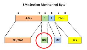
- OTUk SMOH (Section Monitoring Overhead) data
- All remaining OTUk payload data (e.g., the ODUk/OPUk data).

This data will not include the FAS, MFAS nor FEC fields.

Data that is output via this signal, will be aligned with one of the edges of the CI_CK clock output signal. The system designer will typically route this signal to the CI_D input to the downstream OTUk_TT_Sk function.
CI_CKOutputOTUk Characteristic Information - Clock Output:
As the OTUk_CP interface outputs data via the CI_D, CI_FS, CI_MFS and CI_SSF outputs; all of this data will be updated on one of the clock-edges of this clock output signal.
CI_FSOutputOTUk Characteristic Information - Frame Start Output:
The OTUk_CP Interface will pulse this output signal HIGH (for one CI_CK clock period) whenever the OTUk_CP interface outputs the very first bit (or byte) of a new OTUk frame, via this CI_D output.

This output signal will pulse HIGH once for each OTUk frame.
CI_MFSOutputOTUk Characteristic Information - Multiframe Start Output:
The OTUk_CP Interface will pulse this output signal HIGH (for one CI_CK period) whenever the OTUk_CP Interface outputs the very first bit (or byte) or a new OTUk multi-frame via the CI_D output.

This output signal will pulse HIGH once for each OTUk Multi-frame (or one for every 256 OTUk frames).
CI_SSFOutputOTUk Characteristic Information - Server Signal Failure Output:
The OTUk_CP Interface will assert this signal anytime the OTSi/OTUk-a_A_Sk function is declaring a service-affecting defect with the data that it is receiving via the AI_D input).

The OTUk_CP Interface will assert this output signal, whenever the OTSi/OTUk-a_A_Sk function is declaring any of the following defects.
- dLOF
- dLOM
- dAIS
- AI_TSF (if the upstream circuitry is driving the AI_TSF-P input pin, to this function, HIGH).
OTSi/OTUk-a_A_Sk_MP
Interface
MI_FECEnInputManagement Interface - OTSi/OTUk-a_A_Sk FEC Decoding Enable/Disable Input:
This input pin permits the function user to either enable or disable FEC Decoding within the OTSi/OTUk-a_A_Sk function.

Setting this input HIGH enables FEC Decoding.

Setting this input LOW disables FEC Decoding.

If the FEC Decoder is enabled, then it will use the FEC field to correct most symbol errors within the incoming OTUk data-stream (via the AI_PLD input).
MI_pFECcorrErrOutputManagement Interface - FEC Corrected Symbol Count Output:
This output port reflects the number of symbol errors that the OTSi/OTUk-a_A_Sk function has corrected via the FEC Decoder.

This is a Performance Monitoring feature within the OTSi/OTUk-a_A_Sk function.

NOTE: This output pin is INACTIVE if the MI_FECEn input pin is set low (to disable the FEC Decoder).
MI_cLOMOutputManagement Interface - Loss of Multiframe (Correlated) Output Indicator:
This output pin indicates if the OTSi/OTUk-a_A_Sk function is currently declaring the dLOM defect.

If this input pin is LOW, then it indicates that the function is NOT currently declaring the dLOM defect condition.

Conversely, if this input pin is HIGH, then it indicates that the function is currently declaring the dLOM defect condition.

Please see the dLOM defect post for more information on this topic.
MI_cLOFOutputManagement Interface - Loss of Frame (Correlated) Output Indicator:
This output pin indicates if the OTSi/OTUk-a_A_Sk function is currently declaring the dLOF defect.

If this output pin is LOW, then it indicates that the function is NOT currently declaring the dLOF defect condition.

Conversely, if this output pin is HIGH, then it indicates that the function is currently declaring the dLOF defect condition.

Please see the blog post on the dLOF defect for more information on this topic.
MI_cLOSOutputManagement Interface - Loss of Signal (Correlated) Output Indicator:
This output pin indicates if the OTSi/OTUk-a_A_Sk function is currently declaring the dLOS defect.

If this output pin is LOW, then it indicates that the function is NOT currently declaring the dLOS defect.

Conversely, if this output pin is HIGH, then it indicates that the function is currently declaring the dLOS defect condition.

Please see the blog post on the dLOS defect, for more information about this topic.

Has Inflation got You Down? Our Price Discounts Can Help You Fight Inflation and Help You Become An Expert on OTN!! Click on the Banner Below to Learn More!!

Discounts Available for a Short Time!!

Other OTN-Related Posts

Click on the Image below to see more OTN-Related Posts in this blog.

OTN Related Blog

OTN Related Topics within this Blog

OTN Related Topics within this Blog General Topics Consequent Equations - What are they and How can you use them? ...

OTUk-Backward Defect Indicator

This post defines and describes the Backward Defect Indicator (dBDI) defect for the OTUk Layer


What is the dBDI (Backward Defect Indicator) defect at the OTUk Layer?

In short, the dBDI (or Backward Defect Indicator) signal is functionally equivalent to the RDI (Remote Defect Indicator) for OTN applications.

In OTN applications, Network Equipment can declare the dBDI defect at either the OTUk Layer or the ODUk Layer.

This post will discuss the dBDI defect for the OTUk Layer, which we can call the OTUk-BDI defect condition.

We address the dBDI defect for the ODUk Layer in another post.

In another post, I’ve also described the RDI (Remote Defect Indicator) signal or defect in generic terms.

In this post, we are going to describe the following items.

  • What conditions will cause an OTUk Network Element to transmit the dBDI indicator to the remote Network Element?
  • How does the OTUk Network Element transmit the dBDI indicator to the remote Network Equipment?
  • How does the OTUk Network Element receiving the dBDI signal detect and declare the dBDI defect condition?
  • And, how does the OTUk Network Element clear the dBDI defect condition?

Has Inflation got You Down? Our Price Discounts Can Help You Beat Inflation and Help You Become an Expert on OTN!!! Click on the Banner Below to Learn More!!

Corporate Discounts Available!!

What conditions will cause an OTUk Network Element to transmit the dBDI indicator?

In Figure 1, we illustrate two Network Elements (consisting of OTUk Framers and OTUk Transceivers) exchanging OTUk traffic over Optical Fiber.

We will call one of these Network Elements NETWORK ELEMENT WEST and the other Network Element, NETWORK ELEMENT EAST.

NETWORK ELEMENT WEST contains the following pieces of hardware

  • OTUk Framer West
  • OTUk Transceiver East and
  • Optical I/F Circuitry (O->E)/(E->O)

Likewise, NETWORK ELEMENT EAST contains the following pieces of hardware.

  • OTUk Framer East
  • OTUk Transceiver East and
  • Optical I/F Circuitry (O -> E)/(E -> O)

Normal Condition - Network Element West and East

Figure 1, Illustration of two Network Elements that are connected over Optical Fiber

A Defect Condition

Now, let us imagine that some impairment occurs in the span of Optical Fiber carrying OTUk traffic from NETWORK ELEMENT WEST to NETWORK ELEMENT EAST.

This impairment will then cause NETWORK ELEMENT EAST to declare a service-affecting defect, as shown in Figure 2.

Network Element East declares Service Affecting Defect

Figure 2, Illustration of NETWORK ELEMENT EAST declaring a Service-Affecting Defect due to an impairment in Optical Fiber

NETWORK ELEMENT EAST might respond to this defect condition in several ways.  It might transmit the ODUk-AIS indicator towards downstream equipment (as a replacement signal).

NETWORK ELEMENT EAST might also invoke Protection Switching (if supported).

Sending the OTUk-BDI Indicator in Response

Finally, NETWORK ELEMENT EAST will also respond to this defect by transmitting the dBDI (or OTUk-BDI) indicator back towards the upstream Network Element (NETWORK ELEMENT WEST, in this case).

Figure 3 shows an illustration of NETWORK ELEMENT EAST, transmitting the OTUk-BDI indicator (back towards NETWORK ELEMENT WEST) in response to it declaring this service-affecting defect.

Network Element East sends OTUk-BDI signal to Network Element West

Figure 3, Illustration of NETWORK ELEMENT EAST responding to the Defect Condition by sending the OTUk-BDI indicator back towards NETWORK ELEMENT WEST

NETWORK ELEMENT EAST sends the OTUk-BDI indicator (back to NETWORK ELEMENT WEST) to alert it of this defect condition (between the two Network Elements).

In other words, NETWORK ELEMENT EAST is saying, “Hey, NETWORK ELEMENT WEST, I’m having problems with the data that you are sending me.  I’d just thought that I’d let you know”.

There are many reasons why all of these notifications are useful.

This notification gives the Overall Network a clearer picture of exactly where the problem (or impairment) is.

It can also notify maintenance personnel of these problems and provide them with helpful information before they “roll trucks.”

Clueless about OTN? We Can Help!!! Click on the Banner Below to Learn More!!

Discounts Available for a Short Time!!

So What EXACTLY are those Defects that will cause a Network Element to transmit the OTUk-BDI indicator?

The Network Element will transmit the OTUk-BDI indicator anytime it declares any service-affecting defect conditions.

(*) – Must be a member of THE BEST DARN OTN TRAINING PRESENTATION…PERIOD!!!  to see this material.  

The Network Element will continue to transmit the OTUk-BDI indicator for the duration it declares any of these defects.

Once the Network Element no longer declares these defect conditions, it will stop transmitting the OTUk-BDI indicator.

NOTE: ITU-T G.798 is the standards document that specifies the conditions and set of defects that will cause the Network Element to transmit the OTUk-BDI indicator to the remote terminal.

If you wish to see a detailed analysis of how ITU-T G.798 specifies these requirements, please look at the standards document itself or check out the OTUk-BDI – ITU-T G.798 Analysis post.

How does the OTUk Network Element transmit the dBDI indicator?

The Network Element will send the OTUk-BDI indicator by setting the BDI bit-field (Bit 5) within the SM (Section Monitoring) Byte, to  1, within each outbound OTUk frame.

The SM byte resides within the 3-byte SM (Section Monitoring) field of the OTUk Overhead.

Figures 4a, 4b, and 4c present the location of the BDI field.
Figure 4a presents an illustration of the SM-field within the OTUk Overhead.

OTUk Overhead with SM Field Identified

Figure 4a, The SM Field within the OTUk Overhead

Further, Figure 4b illustrates the SM byte’s location within the 3-byte SM Field (within the OTUk Overhead).

SM field with the SM Byte identified

Figure 4b, The SM-Byte within the SM Field

Finally, Figure 4c shows the location of the BDI-field within the SM-byte (within the SM-field of the OTUk Overhead).

SM Byte with OTUk-BDI field identified

Figure 4c, The Location of the BDI bit-field within the SM Byte, within the SM Field, within the OTUk Overhead

Likewise, the Network Element will end its transmission of the OTUk-BDI indicator by setting the BDI bit-field back to “0” within each outbound OTUk frame.

How does the OTUk Network Element detect and declare the dBDI indicator?

In the scenario that we described above (via Figure 3), NETWORK ELEMENT EAST will continue to transmit the OTUk-BDI signal to NETWORK ELEMENT WEST as long as it (NETWORK ELEMENT EAST) declares the service-affecting defect within its Ingress (Receive) signal.

If NETWORK ELEMENT WEST receives the OTUk-BDI indicator within at least five (5) consecutive OTUk frames, it will declare the dBDI defect condition.

In other words, if NETWORK ELEMENT WEST (or any Network Element) were to receive at least five (5) consecutive OTUk frames, in which the BDI bit-field is set to “1”, then it will declare the dBDI defect.

Figure 5 illustrates NETWORK ELEMENT WEST declaring the dBDI defect after receiving five consecutive OTUk Frames with the SM-BDI field set to “1”.

Network Element West declares the dBDI defect condition

Figure 5, Illustration of NETWORK ELEMENT WEST declaring the dBDI defect condition

How does the OTUk Network Element clear the dBDI defect condition?

Whenever NETWORK ELEMENT EAST has determined that the service-affecting defect (which caused it to transmit the dBDI signal in the first place) is cleared, it will stop sending the dBDI signal back out to NETWORK ELEMENT WEST.

NETWORK ELEMENT EAST will stop sending the dBDI signal by setting the BDI bit-field (within the SM field) to “0” within each outbound OTUk frame.

If NETWORK ELEMENT WEST (which is currently declaring the dBDI defect condition) were to receive at least five (5) consecutive OTUk frames, in which the BDI bit-field is set to “0”, then it will clear the dBDI defect.

Figure 6 illustrates NETWORK ELEMENT WEST clearing the dBDI defect after receiving five consecutive OTUk Frames with the SM-BDI field set to “0”.

Network Element East declares Service-Affecting Defect

Figure 6, Illustration of NETWORK ELEMENT WEST clearing the dBDI defect condition

Monkey Pox and Covid? It’s Scary Out There. We Can Help You Become an Expert on OTN Before It’s Safe to Venture Out!! Click on the Banner Below to Learn More!!

Discounts Available for a Short Time!!

For More Information on OTN Posts in this Blog, click on the Image below.

OTN Related Blog

OTN Related Topics within this Blog

OTN Related Topics within this Blog General Topics Consequent Equations - What are they and How can you use them? ...

What is the OTUk-AIS Indicator?

This post defines and describes the OTUk-AIS signal for OTN applications.


What is the OTUk-AIS Maintenance Signal?

What exactly is an OTUk-AIS signal?

AIS is an acronym for Alarm Indication Signal.

Another post describes the role/function of AIS.

Whenever an OTN Network Equipment (NE) transmits an OTUk-AIS signal, it generates and transmits an Unframed PN-11 (e.g., PRBS11) Pattern.

More specifically, ITU-T G.709 defines this PN-11 sequence by the generating polynomial:  1 + x9 + x11.

Since this is an Unframed signal, then this means that all of the OTUk, ODUk, and OPUk overhead fields (within the OTUk signal) will be overwritten with this PN-11 pattern.

Figure 1 presents a simple illustration of an OTUk-AIS signal.

OTUk-AIS Pattern

Figure 1, Simple Illustration of an OTUk-AIS signal.

What are the timing/frequency requirements for an OTUk-AIS signal?

The OTN NE will need to transmit this signal at the same nominal bit rate as an ordinary OTUk signal.

Like any ordinary OTUk signal, the OTN STE will need to transmit this data at the nominal bit-rate ± 20ppm.

Table 1 presents the nominal bit-rates for the OTUk signals (and, in turn, for the OTUk-AIS signal) for each value of k.

Table 1, Required Bit Rates for the OTUk-AIS signal.

OTUk Bit Rate

Does the OTN NE need to align the PN-11 pattern sequence with the OTUk frame?

In short, the answer is No.

The length of the PN-11 sequence is 2047 bits (e.g., 211 – 1).  And the capacity of a given OTUk frame is 130,560 bits.

Since the numeral 130,560 is NOT an integral multiple of 2047, the PN-11 sequence will cross OTUk frame boundaries.

When would OTN Network Equipment transmit/generate an OTUk-AIS signal?

For the time being, ITU-T G.709 has not defined a set of conditions (or defects) upon which the OTN STE would transmit the OTUk-AIS signal.

ITU-T G.709 has reserved this type of signal as a placeholder for future use.

The standards committee may (at a later time) specify a set of conditions upon which an OTN STE would transmit the OTUk-AIS signal.

Additionally, ITU-T G.709 is NOT requiring that OTN Equipment or Chip Vendors design their products to be capable of generating/transmitting the OTUk-AIS signal.

However, ITU-T G.709 mandates that OTN Equipment and Chip Vendors be capable of receiving, detecting, and flagging the OTUk-AIS pattern.

Click HERE for Information on How an STE does declare and clear the dAIS (OTUk-AIS) defect condition.

Why are we even talking about an OTUk-AIS Signal if we are NOT currently required to generate it?

Once again, the Standards Committee has reserved this signal for FUTURE USE.

They envision defining conditions for which an OTN Section Terminating Equipment (STE) would generate and transmit the OTUk-AIS signal in a system application.

Is there another type of AIS signal that OTN APPLICATIONS ARE ACTIVELY USING?

Yes, ITU-T G.709 also recommends the use of ODUk-AIS.  OTN Path Terminating Equipment is actively using the ODUk-AIS indicator.

Has Inflation got You Down? Our Price Discounts Can Help You Fight Inflation and Help You Become an Expert on OTN!! Click on the Banner Below to Learn More!!

Temporary Discount Offered!!

For More Information on OTN Posts in this Blog, click on the Image below.

OTN Related Blog

OTN Related Topics within this Blog

OTN Related Topics within this Blog General Topics Consequent Equations - What are they and How can you use them? ...

What is AIS (Alarm Indication Signal)?

This post defines and describes the AIS (Alarm Indication Signal). It also describes how and when Network Equipment will transmit this type of signal.


What is an AIS (Alarm Indication Signal)?

What does the term AIS Mean?

AIS is an acronym for Alarm Indication Signal.

Where is the AIS Signal Used?

The AIS signal is a particular type of alarm (or maintenance) signal that a Network Element (within a Telecom/Datacom application) will generate and transmit (in its downstream path) anytime it detects some service-affecting defect upstream.

For example:

Suppose a Network Element (NE) was to declare the LOS (Loss of Signal) or the LOF (Loss of Frame) defect within its incoming telecom/datacom signal. In that case, it will respond to this defect condition by transmitting the AIS signal downstream.

Whenever the Network Element transmits this AIS signal downstream, it is (in effect) replacing its defective incoming signal with the AIS signal.

What EXACTLY is an AIS signal?

The exact pattern/signature of an AIS signal depends upon the telecom/datacom standard and network layer we use.

For some datacom/telecom standards, the AIS signal is transmitted (and received) as an Unframed All One’s pattern.

In other standards, we will transmit the AIS indicator as a Framed All One’s pattern (e.g., where the framing alignment fields still use typical values, but the payload fields are filled with an All One’s pattern).

Finally, the OTUk AIS pattern is an Unframed PN-11 (PRBS11) pattern.

In all cases, the NE will generate and transmit the AIS signal at the nominal line rate (of the customarily transmitted signal).

The frequency accuracy requirements for this AIS signal also depend on the governing standards for the Telecom/Datacom system.

I have included posts that define the AIS patterns for OTUk and ODUk types of signals (for OTN applications).

When do we transmit the AIS pattern?

We will go through a couple of examples to illustrate how and when we will transmit the AIS signal.

Example # 1 – The Unerred/Normal Condition

Figure 1 presents a straightforward illustration of a portion of a 3R Repeater/Regenerator, which consists of the following components:

  • Two (2) Receive Line Interface blocks (one block is labeled W for West, and the other block is labeled E for East)
  • Two (2) Receive Framer blocks (W – West and E – East)
  • Two (2) Transmit Line Interface blocks (W – West and E – East)
  • Two (2) Transmit Framer blocks (W – West and E – East)
  • CS (Clock Smoothing/Jitter Attenuation) PLL (Phase-Locked Loop)
  • AIS OSC (Stand-Alone Oscillator).
  • FIFO/Buffer
  • Two (2) Defect Decoder blocks (W – West and E – East)

In this figure, our 3R Repeater/Regenerator receives a good (error-free) signal from the “West Terminal.”

The 3R Repeater/Regenerator will first receive this signal through its Receive Line Interface (W) block.

Afterward, this signal passes through to the Receive Framer (W) block.

Suppose the Receive Line Interface (W) and the Receive Framer (W) blocks were to detect no problems within this signal. In that case, the 3R Repeater/Regenerator will allow this signal to pass through the Transmit Framer (E) and Transmit Line Interface (E) blocks as is.

Our 3R Repeater/Regenerator will transmit this same data to the East Terminal.

Additionally, the Transmit Framer (E) and Transmit Line Interface (E) blocks would transmit the outbound data (towards the East Terminal) based upon the Recovered Clock signal (which originated from the West Terminal and has been routed through the Clock Smoothing PLL for Jitter Attenuation purposes).

Figure 1 presents an illustration of this Normal (No Defect) Condition.

Portion of 3R Repeater/Regenerator during Normal Operation

Figure 1, Illustration of the 3R Repeater/Regenerator – during Good/Normal Conditions.

Please note that I have grayed out the non-relevant portions of Figure 1 so we can focus our discussion on this Defect Declaration to AIS Generation mechanism in the West-to-East Terminal Path.

Now we will illustrate the case where we will transmit the AIS indicator.

Example # 2 – The dLOS/Abnormal Condition

Figure 2 presents another straightforward illustration of a 3R Repeater/Regenerator.

However, in this figure, there is an impairment in the signal that originates from the West Terminal such that our Network Element is now declaring the dLOS (Loss of Signal) defect with this signal.

It is possible that a backhoe or some other mishap severed this signal.

Nonetheless, our 3R Repeater/Regenerator is no longer receiving its signal from the West Terminal.

This also means that our 3R Repeater/Regenerator has no data to send to the East Terminal.

In this situation, our 3R Repeater/Regenerator will respond by doing the following things.

The Receive Line Interface (W) or the Receive Framer (W) blocks will declare the dLOS (Loss of Signal) defect with the signal that it is receiving from the West Terminal.

The Transmit Framer (E) and Transmit Line Interface (E) (which resides directly behind the Receiving Line Interface and Framer blocks – that are declaring the dLOS condition) will proceed to transmit the AIS indicator (to the East Terminal) as a replacement signal for the signal that we are no longer receiving from the West Terminal.

Additionally, the Transmit Framer (E) and Transmit Line Interface (E) blocks would transmit the AIS pattern (towards the East Terminal) based upon the output frequency of the AIS Oscillator (which is a stand-alone oscillator – that operates at the specified line-rate/clock frequency).

Figure 2 illustrates the dLOS/AIS Transmission Condition for our 3R Regenerator/Repeater.

3R Repeater/Regenerator declaring dLOS and transmitting AIS

Figure 2, Illustration of the 3R Repeater/Regenerator – during the dLOS/Abnormal Condition.

The Transmit Framer (E) and Transmit Line Interface (E) blocks will continue to transmit the AIS indicator to the East Terminal for the duration that the Receive Line Interface (W) and the Receive Framer (W) blocks are declaring the dLOS defect with the signal that they are receiving from the West Terminal.

The Transmit Framer (E) and Transmit Line Interface (E) blocks will cease to transmit the AIS indicator once the Receive Line Interface (W) and the Receive Framer (W) blocks clear the dLOS defect and start to receive good/normal data from the West Terminal.

At this point, the Transmit Framer (E) and Transmit Line Interface (E) blocks will transmit good/normal data to the East Terminal.

In addition to the dLOS defect, the Network Element will typically transmit the AIS indicator (downstream) in response to the following other defects.

  • dLOF (Loss of Frame Defect)
  • dLOM (Loss of Multi-Frame Defect)
  • dLOFLANE (Loss of Frame of Logical Lane) – for OTL3.4 or OTL4.4 applications (*)
  • dLOL (Loss of Lane Alignment) – for OTL3.4 or  OTL4.4 applications (*)
  • dTIM (Trail Trace Identifier Mismatch)

(*) – Need to be a member of THE BEST DARN OTN TRAINING PRESENTATION…PERIOD!!! to access these links.

Why do we bother to transmit the AIS signal as a replacement signal?

We transmit the AIS indicator downstream in response to service-affecting defects for several reasons.

I will list some of those reasons below.

  • Alerts downstream equipment that we have detected and declared a service-affect defect upstream.
  • To suppress (or prevent) the downstream equipment from declaring their service-affecting defect.
  • Aids in troubleshooting and system debugging. It is easier to isolate the causes of defect conditions if we know exactly which NE is declaring the defect and not the whole chain of NEs downstream.
  • The downstream Receive Circuitry provides a much-needed clock signal at the correct bit rate. Clock Recovery PLLs (Phase-Locked-Loops) and Bias Controllers (for Optical Receive circuitry) all need upstream NEs to provide them with a line signal with the appropriate timing (bit-rate).

The AIS signal accomplishes these goals.

Has Inflation got You Down? Our Price Discounts Can Help You Fight Inflation and Help You Become an Expert on OTN!! Click on the Banner Below to Learn More!!!

Discount Available Temporarily