What is the Byte-Format of the APS/PCC Field for Linear Protection Switching Applications within the OTN

This blog post briefly defines and describes the Nibble and Byte fields of the APS/PCC field, for Linear-Protection-Switching and OTN Applications.

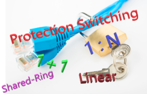
Introduction to the APS/PCC Field

This blog post aims to define and describe the byte format of the APS/PCC field within the ODU Overhead whenever we support Linear Protection Switching applications within the OTN. ITU-T G.873.1 specifies the byte/nibble format of the APS/PCC field that we use within the OTN for Linear Protection Switching.

Whenever the System Designer needs to support the following:

  • Linear Protection Switching within the Optical Transport Network (defined within ITU-T G.709)
  • An APS Communication Protocol (because the user is either using the 1:N Protection Architecture or Bidirectional Switching

Then the user will need to use the APS/PCC (Automatic Protection Switching/Protection Control Communications) channel (and field) to support the APS protocol.

The APS/PCC field resides within the ODU Overhead, as I show below in Figure 1.

Location of APS/PCC field within the ODU Overhead

Figure 1, Location of the APS/PCC Field within the ODU Overhead of an OTU Frame.

Figure 1 shows that the APS/PCC field resides within the fourth row and the fifth through eighth-byte position within an OTU frame. The length of the APS/PCC field is four bytes wide.

Whenever we are designing OTN networks to also support protection switching (and using the APS Communications Protocol) in the process, then we will use the APS/PCC field to transport APS Messages from one Network Element to another.

Byte/Nibble Format of the APS/PCC Field

I show the Byte/Nibble format of the APS/PCC field below in Figure 2.

APS/PCC Field Format for Linear Protection Switching Applications

Figure 2, Byte/Nibble format of the APS/PCC Field

Figure 2 shows that the APS/PCC field consists of the following Nibbles and Byte-fields:

Request/State Nibble (Bits 1-4)

The purpose of this Nibble-field is to either:

  • Transmit Protection-Switching commands or requests to the remote terminal of the Protection-Group, or
  • Transmit information about Defect Conditions or States.

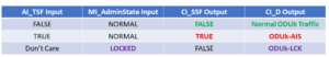
Table 1 presents a list of values (within the Request/State Nibble field) and their corresponding Meaning.

Table 1, Standard Values within the Request/State Nibble field and their Corresponding Meaning.

Meaning of Request State Nibble field of APS/PCC Field - Linear Protection Applications

So, for example, if a given Protection Switching terminal needs to transmit the SF Command, it would set the Request/State Nibble (within its outbound APS Message) to [1, 1, 0, 0], as I show in Table 1.

Protection Type Nibble (Bits 5 – 8)

The Protection Type Nibble field occupies the second set of four bits of the APS/PCC field.

The purpose of this nibble-field is to communicate (to the remote end of the Protection Group) many of the governing parameters of our Protection-Switching scheme.

The following table presents a list of the bit-fields within the Protection-Type Nibble and their meaning/description.

Table 2, A List of the Bit-Fields, within the Protection-Type Nibble and their Meaning/Description

Protection Type Nibble of APS/PCC field
Bit A – APS Channel

This bit-field indicates if the Protection Group is either supporting an APS Communication Protocol or not, as I describe below.

  • 0 = No APS Channel (Not using the APS Communication Protocol)
  • 1 = APS Channel (We are using the APS Communication Protocol)
Bit B – Bridge (Permanent)

This bit-field indicates if the Protection Group supports the 1+1 or 1:N Protection Architecture, as I show below.

Bit D – Directional Switching

This bit-field indicates if the Protection Group supports Unidirectional or Bidirectional Switching, as shown below.

  • 0 = Unidirectional Switching
  • 1 = Bidirectional Switching
Bit R – Revertive Operation

This bit-field indicates if the Protection Group supports the Revertive or Non-Revertive Operation, as I show below.

  • 0 = Non-Revertive Operation
  • 1 = Revertive Operation

Requested Signal Byte – APS/PCC Field – Byte 2

The Requested Signal byte-field identifies the signal that the Near-End (e.g., the Requesting Terminal) requests to be carried over to the Protection Transport Entity.

Ultimately, we a request at the Far-End Terminal to place the Requested Signal on the Protection Transport Entity, following this Protection Command.

For the 1+1 Protection Architecture

For the 1+1 Protection Architecture, the Protection-Switching Terminal should set this byte-field to “0x01” (for most APS Commands) to denote Normal Traffic Signal # 1. Normal Traffic Signal # 1 is typically the ONLY Normal Traffic Signal in a given direction for a 1+1 Protection Switching Architecture.

For the 1:N Protection Architecture

If the Requesting Terminal wishes to command the remote end to bridge the NULL Test Signal to the Protection Transport entity, it should set this byte-field to 0x00 when issuing an APS command.

Likewise, suppose the Requesting Terminal wishes to command the remote end to bridge the Extra Traffic Signal to the Protection Transport entity. In that case, it should set this byte-field to 0xFF when issuing an APS command.

Finally, suppose the Requesting Terminal wishes to command the remote end to bridge a Normal Traffic Signal to the Protection Transport entity. During a Protection Switching event, it should set this byte-field to the appropriate number (corresponding with the defective Normal Traffic Signal). Valid Numbers for the Requested Byte value range from 0x01 to 0xFE, depending upon which Normal Traffic signal requires Protection-Switching.

Table 2 lists the appropriate Requested Signal Values for the 1:N Protection Architecture.

Table 2, List of Appropriate Requested Signal Values for the 1:N Protection Architecture

Requested Signal Byte Meaning - APS/PCC Field

Bridged Signal Byte – APS/PCC Field – Byte 3

For this field, the REQUESTING terminal will set this byte-field to the value that identifies which signal this terminal is currently bridging to the Protection Transport entity.

For the 1+1 Protection Architecture


When using the 1+1 Protection Architecture, the Protection-Switching Terminal should set this byte-field to “0x01” (for most APS Commands) to denote Normal Traffic Signal # 1. Normal Traffic Signal # 1 is typically the ONLY Normal Traffic Signal in a given direction for a 1+1 Protection Switching Architecture.

For the 1:N Protection Architecture

If the Requesting Terminal is bridging the NULL Test Signal to the Protection Transport entity, it must set this byte-field to 0x00 when issuing an APS command. The Requesting Terminal tells the remote terminal that it is bridging the NULL Test Signal to the Protection Transport entity.

Likewise, if the Requesting Terminal is bridging the Extra Traffic Signal to the Protection Transport entity, it must set this byte-field to 0xFF when issuing an APS command.

Finally, suppose the Requesting Terminal is currently implementing Protection Switching and is bridging one of the Normal Traffic Signals to the Protection Transport entity. In that case, it must identify that Normal Traffic Signal by setting this byte-field to the appropriate number (corresponding with the defective Normal Traffic Signal). Valid Numbers for the Requested Byte value range from 0x01 to 0xFE, depending upon which Normal Traffic signal requires Protection-Switching.

Table 3 presents a list of the appropriate Bridged Signal Values for the 1:N Protection Architecture.

Table 3, List of Appropriate Bridged Signal Values for the 1:N Protection Architecture

Bridged Signal Byte Meaning - APS/PCC Field

Reserved Byte – Byte 4

This byte-field is reserved for future use/standardization.

Clueless About OTN? We Can Help!! Click Below to Learn More!!

Example of Using the APS/PCC Field for the 1+1 Protection Architecture

Let’s suppose we use the 1+1 Protection Architecture within our Protection Scheme. Further, let’s assume that one of the Network Elements declares the SF_W (Signal Fail within the Working Transport Entity) condition, as shown below in Figure 3.

SF Declared in Normal Traffic Signal # 2 - 1+1 Protection Architecture

Figure 3, Tail-End Circuit at NE Z declares the SF_W Condition.

NE Z Sends the SF_W APS Message to NE A

In this case, NE Z (the Network Element declaring the SF_W Condition) will need to send the SF_W APS Command to the remote terminal. I show this APS Command below in Figure 4.

NE Z sends SF_W APS Command to NE A - 1+1 Protection Architecture

Figure 4, NE Z sending the SF_W APS Command to NE Z.

Please note that (within this APS Command) NE Z is setting the Request Command to [1, 1, 0, 0] to denote that it is transmitting the SF Command.

Further, NE Z is also setting the Protection Type Nibble to information NE A, which is operating with the following Protection-Switching characteristics:

  • A = 1: We are using an APS Communication Protocol
  • B = 0: We are using a Permanent Bridge (for a 1+1 Protection Architecture)
  • D = 1: We are supporting Bidirectional Switching, and
  • R = 1: We are supporting Revertive Switching

Next, NE Z is setting the Requested Byte to “0x01”. This setting denotes two things:

  • First, we are declaring the SF condition within the Working Transport Entity. If we set the Requested Byte to “0x00”, this would denote that we are declaring the SF condition with the Protection Transport entity.
  • Second, we are requesting that the remote terminal (NE A, within Figure 4) should bridge the Normal Traffic Signal (Signal # 0x01) to the Protection Transport entity. (NOTE: Because this is the 1+1 Protection Architecture, we are already permanently bridging the Normal Traffic Signal (0x01) to the Protection Transport entity.

Finally, NE Z is setting the Bridged Byte to “0x01”. This setting denotes that we are already bridging the Normal Traffic Signal (0x01) to the Protection Transport Entity. The Permanent Bridge is inherent to the 1+1 Protection Architecture.

Subsequent APS Commands

NE A and NE Z will exchange more APS Commands to deal with this instance of the SF condition. I’m only showing the initial request from NE Z to NE A.

Example of Using the APS/PCC Field for the 1:N Protection Architecture

Let’s suppose we are using the 1:N Protection Architecture within our Protection Scheme. Further, let’s assume that one of the Network Elements declares the SF_W Condition with Working Transport Entity # 2, as I show below in Figure 5.

SF Declared in Normal Traffic Signal # 2 - 1:N Protection Architecture

Figure 5, Tail-End Circuit at NE Z declares the SF_W Condition for Working Transport Entity # 2.

NE Z Send the SF (within Normal Traffic Signal # 2) Message to NE A

In this case, NE Z (the Network Element declaring the SF_W Condition) will need to send the SF_W APS Command to the remote terminal. I show this APS Command below in Figure 6.

NE Z sends SF_W APS Command to NE A - 1:N Protection Architecture

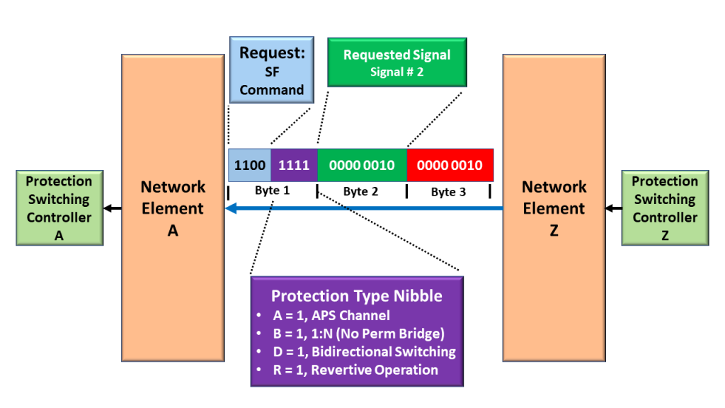
Figure 6, NE Z sending the SF_W APS Command to NE Z.

Please note (again) that (within this APS Command) NE Z is setting the Request Command to [1, 1, 0, 0] to denote that it is transmitting the SF Command.

Further, NE Z is also setting the Protection Type Nibble to information NE A, which is operating with the following Protection-Switching characteristics:

  • A = 1: We are using an APS Communication Protocol
  • B = 1: We are using a Non-Permanent Bridge (for a 1:N Protection Architecture)
  • D = 1: We are supporting Bidirectional Switching, and
  • R = 1: We are supporting Revertive Switching

Next, NE Z is setting the Requested Byte to “0x02”. This setting denotes two things:

  • First, we are declaring the SF condition within the Working Transport Entity. If we set the Requested Byte to “0x00”, this would denote that we are declaring the SF condition with the Protection Transport entity.
  • Second, we are requesting that the remote terminal (NE A, within Figure 5) should bridge the Normal Traffic Signal # 2 (Signal # 0x02) to the Protection Transport entity. We are declaring the defect with Working Transport Entity # 2. We need to alert the remote terminal that we need to bypass this signal path.

Finally, NE Z is setting the Bridged Byte to “0x02”. This setting denotes that we are already bridging the Normal Traffic Signal # 2 (0x02) to the Protection Transport Entity.

Subsequent APS Commands

NE A and NE Z will exchange more APS Commands to deal with this instance of the SF condition. I’m only showing the initial request from NE Z to NE A.

More Information/Training

If you wish for more information/training on this topic, then check out the video on the APS Communication Protocol (*).

(*) – Requires membership to access.

Has Inflation got You Down? Our Price Discounts Can Help You Fight Inflation and Help You Become an Expert in OTN!! Click on the Banner Below for More Details!!

Click on the Image Below to see more Protection-Switching related content on this Blog:

Protection-Switching Related Blog

Protection-Switching Related Blog Posts

Protection-Switching Related Blog Posts Basic Protection-Switching Terms Head-End (Source Node) Hold-Off Timer Protection-Group Protection-Transport entity Selector Switch Tail-End (Sink Node) ...

What is the pF_DS (Far-End Defect Second) Performance-Monitoring Parameter for the ODUk Layer?

This blog post breifly defines the pF_DS (Far-End Defect Second) Performance Monitoring paramteter that the OTN PTE will compute and generate.

This blog post aims to briefly define and describe the pF_DS (Far-End Defect Second) Performance Monitoring parameter that the OTN PTE (or ODUk_TT_Sk Atomic Function) will compute and generate.

The OTN PTE (or ODUk_TT_Sk function) will include information on pF_DS without each Performance Monitoring report that it sends to System Management.

Performance Monitoring Reports

NOTES:

  1. The OTN STE (OTUk_TT_Sk Atomic Function) also monitors and generates information on the pF_DS (Far-End Defect Second) parameter at the OTUk Layer. Please see the pF_DS at OTUk Layer Post for more details on this parameter.
  2. Throughout this post, I will use the terms: OTN PTE and ODUk_TT_Sk Function interchangeably. In the context of this blog post, these two terms mean the same thing.

Introduction

At the ODUk Layer, the OTN (Sink) PTE is the entity that is responsible for detecting and reporting Far-End Defect Second events.

As the OTN PTE receives and monitors its incoming ODUk signal, it will check for many things. It will continuously check for the incoming ODUk signal for Service-Affecting Defect (e.g., dAIS, dOCI, dLCK, dTIM, etc.) as well as bit (or symbol) errors (e.g., PM-BIP-8 errors and PM-BEI errors).

Another thing that the OTN PTE will do (as it continuously monitors its incoming ODUk signal) is to divide each second of (monitoring) time into the following two categories:

  • Far-End Available (Working) Seconds, and
  • Far-End Defect Seconds

Anytime the OTN PTE detects and categorizes a given one-second period as being a Far-End Defect Second, it will increment the pF_DS parameter and report that information to System Management.

New Comprehensive OTN Training…. Available Now. Click on the Banner Below to Learn More!!

Discounts Available for a Short Term!!

So When does the OTN PTE detect and flag a given One-Second Period as being a “Far-End Defect Second”?

ITU-T G.798 presents the following Performance Monitoring Equation for the ODUk_TT_Sk function.

pF_DS <- dBDI

Where:

dBDI is the current state of the ODUk-BDI or the Backward Defect Indicator Defect (at the ODUk Layer).

The OTN PTE (or ODUk_TT_Sk function) will continuously evaluate the above equation as it monitors its incoming ODUk signal.

This equation states that the OTN PTE will declare a given one-second period as being a Far-End Defect Second if it has declared the dBDI defect condition during any portion of that one second.

A given OTN PTE will declare a one-second period as a Far-End Defect Second if the remote OTN PTE declares any of the following defect conditions:

  • dAIS (ODU-AIS)
  • dOCI
  • dLCK
  • dTIM

In this case, the OTN PTE will increment the pF_DS parameter for each one-second period it categorizes as a Far-End Defect Second.

Conversely, the OTN PTE will declare a one-second period as an Available Second if the remote OTN PTE is not declaring any of the defects mentioned above. The OTN PTE will NOT increment the pF_DS parameter in this case.

What Does This Mean in English?

Of course, if the OTN PTE declares the dBDI defect condition, then this also means that the remote PTE is declaring a service-affecting defect condition. In other words, the pF_DS parameter reflects the health of the remote (or Far-End) terminal.

If the remote terminal declares no service-affecting defects, the near-end terminal will not increment the pF_DS parameter. On the other hand, if the remote terminal declares a service-affecting defect, then the near-end terminal will increment the pF_DS parameter.

So, if the ODUk_TT_Sk function has declared the dBDI defect condition for even a fraction of a given one-second period, it will declare it as a Far-End Defect Second. It will also set the parameter pF_DS to 1 and report that information to System Management.

Conversely, if the OTN PTE determines that the ODUk_TT_Sk function did not declare the dBDI defect condition at all during a given one-second period. In that case, it will declare that one-second period is a Far-End Available (Working) Second. In this case, the OTN STE will NOT set the parameter pF_DS to 1.

Hence the pF_DS parameter reflects the network’s health at the remote terminal (e.g., the other end of the ODUk Path).

Is there such a thing as a Near-End Defect Second?

Throughout this post, we have used the term: Far-End Defect Second. Does this mean that there is another parameter called Near-End Defect Second?

Answer: Yes, there is such a parameter. See the Near-End Defect Seconds (pN_DS) post at the ODUk Layer for more details.

Clueless about OTN? We Can Help!! Click on the Banner Below to Learn More.

Discounts Available for a Short Time!!

And Finally, Click on the Image Below to see More OTN-Related Topics in this Blog.

OTN Related Blog

OTN Related Topics within this Blog

OTN Related Topics within this Blog General Topics Consequent Equations - What are they and How can you use them? ...

OTN – Lesson 12 – Detailed Discussion of SNC/S Monitoring (Protection Switching)

This blog post presents a video that describes (in detail) SNC/S (Subnetwork Circuit Protection – Sublayer) Monitoring for Protection Switching.

Lesson 12 – Video 7 – Detailed Discussion of SNC/S (Subnetwork Circuit – Sublayer) Monitoring for Protection Switching

This blog post contains a video that presents a detailed discussion of SNC/S (Subnetwork Circuit – Sublayer) Monitoring for Protection Switching purposes at the ODU Layer.

In particular, this video will discuss the following topics:

  • A Detailed Review of SNC/S (Subnetwork Circuit Protection/Sublayer) Monitoring.
  • This video shows example locations/conditions of where we would use SNC/S Monitoring and why we would use this form of monitoring.
  • This video also highlights similarities of SNC/S with SNC/I Monitoring.
  • It also shows the differences between SNC/S and SNC/Ne or SNC/Ns monitoring.
  • Finally, this video reviews a Multi-Administrative Domain Network (and
    Tandem Connection Monitoring) and describes how SNC/S works within a given “Protect Domain.”

Check Out the Video Below.

Continue reading “OTN – Lesson 12 – Detailed Discussion of SNC/S Monitoring (Protection Switching)”

OTN – Lesson 12 – Detailed Discussion of SNC/N Monitoring (Protection Switching)

This blog post presents a video that describes (in detail) SNC/N (Subnetwork Protection – Non-Intrusive) Monitoring for Protection Switching.

Lesson 12 – Video 6 – Detailed Discussion of SNC/N (Subnetwork Circuit – Non-Intrusive) Monitoring for Protection Switching

This blog post contains a video that presents a detailed discussion of SNC/N (Subnetwork Circuit – Non-Intrusive Monitoring, for Protection-Switching purposes, at the ODU Layer.

In particular, this video will discuss the following topics:

  • A Detailed Review of SNC/Ne (Subnetwork Circuit Protection/Non-Intrusive End-to-End) Monitoring, and
  • A Detailed Review of SNC/Ns (Subnetwork Circuit Protection/Non-Intrusive Sublayer) Monitoring.
  • This video shows example locations/conditions of where we would use SNC/Ne or SNC/Ns Monitoring and why we would use this form of monitoring.
  • This video also highlights the similarities and differences between SNC/Ne and SNC/Ns Monitoring.

Check Out the Video Below

Continue reading “OTN – Lesson 12 – Detailed Discussion of SNC/N Monitoring (Protection Switching)”

OTN – Lesson 12 – Detailed Discussion of SNC/I Monitoring (Protection Switching)

This blog post presents a video that describes (in detail) SNC/I (Subnetwork Circuit – Inherent) Monitoring for Protection Switching.

Lesson 12 – Video 4 – Detailed Discussion of SNC/I (Subnetwork Circuit – Inherent) Monitoring for Protection Switching

This blog post contains a video that presents a detailed discussion of SNC/I Monitoring, both at the OTU and ODU layers.

In particular, this video will discuss the following topics:

  • How to perform SNC/I Monitoring at the OTU Layer
    • What Circuitry (Atomic Functions) that we should use
    • What defects to monitor
    • Which is the Normal Traffic Signal when doing SNC/I Monitoring at the OTU Layer.
    • What happens when we declare an OTU Layer Service-Affecting defect (dLOS, dLOF, dLOM, dLOL, dLOFLOM, dLOR, dAIS, and dTIM)?
    • What happens when we declare the SM-dDEG (OTU-layer Signal Degrade) defect?
    • How does protection-switching work?
  • How to perform SNC/I Monitoring at the ODU Layer
    • What Circuitry (Atomic Functions) that we should use
    • What defects to monitor
    • Which is the Normal Traffic Signal when doing SNC/I Monitoring at the ODU Layer.
    • What happens when we declare an ODUk Server-Layer service-affecting defects (such as dAIS, dOCI, dLCK, dTIM, dLOOMFI, and dPLM)?
    • What happens when we declare ODUj Tributary-Layer service-affecting defects (such as dLOFLOM and dMSIM)
    • What happens when we declare the PM-dDEG (ODU-layer Signal Degrade) defect?
    • How does protection-switching work?

Check Out the Video Below

Continue reading “OTN – Lesson 12 – Detailed Discussion of SNC/I Monitoring (Protection Switching)”

Lesson 2 – ODU Framing

This post provides a comprehensive review and video training of the ODU frame and its overhead fields.

Lesson 2 – ODU (Optical Data Unit) Frame Training

This post presents a video that discusses the ODU (Optical Data Unit) Frame in considerable detail.  

In addition to discussing the ODU frame format, this video also discusses the ODU overhead fields and their roles.

Finally, this video discusses special ODUk signals, such as ODU0, ODU2e, and ODUflex.  

Continue reading “Lesson 2 – ODU Framing”

What are Consequent Equations?

This post briefly defines and describes Consequent Equations that ITU-T G.798 uses for OTN Applications.

What are Consequent Equations, and How Should You Interpret Them?  

The purpose of this blog post is two-fold.

  • To describe the concept of Consequent Equations and
  • To discuss how we can use and interpret these Consequent Equations.

Introduction

Many ITU Standards (such as ITU-T G.798 for OTN Applications) will discuss many aspects of defects. These standards will define defects such as dAIS (Alarm Indication Signal) and dLOM (the Loss of Multi-frame).  

These same standards will also define the criteria that an OTN Network Element (be it an STE or PTE) should use to declare or clear a given defect.  

For example, ITU-T G.798 specifies all of the following defects that an OTN STE can declare and clear.

And that’s all well and good.  

NOTE: (*) – Indicates that you need to be a member of THE BEST DARN OTN TRAINING PRESENTATION…PERIOD!!! to access these links.

How should an STE/PTE Respond Whenever it Declares a Defect?  

However, what else should an STE do whenever it declares (for example) the dLOF defect condition?  

Does this STE have a responsibility to notify other STEs of this defect?  

Similarly, what else should a PTE do whenever it declares (for example) the dTIM (ODUk-TIM) defect condition?  

Again, does this PTE have a responsibility to notify other nearby PTEs of this defect?

The short answer to both of these questions is, “Yes, for those specific defects that I mentioned, they do have a responsibility to notify upstream and downstream equipment of the occurrence of those defect conditions.”

However, to confuse things, the PTE/STE must notify upstream and downstream PTE/STE whenever some defects occur, but not others.  

How Do We Sort out This Confusion?  

The Answer:  Consequent Equations.  

Let’s assume that a certain STE is declaring the dLOF Defect condition, as shown below in Figure 1.

Consequent Equation - OTSi/OTUk_A_Sk function declares the dLOF defect

Figure 1, Illustration of the STE (e.g., the OTSi/OTUk-a_A_Sk Atomic Function) declares the dLOF defect condition.

What happens next?

At this point, let’s write down the Consequent Equation that pertains to this STE (or the OTSi/OTUk-a_A_Sk function in this case):

aSSF <- dLOS-P or dAIS or dLOF or dLOM or AI_TSF-P

Where:

aSSF is the current state of the CI_SSF output pin (of the OTSi/OTUk-a_A_Sk function).

dLOS-P is the current state of the Loss of Signal-Path Defect condition

dAIS is the current state of the OTUk-AIS Defect Condition

dLOF is the current state of the Loss of Frame Defect Condition

dLOM is the current state of the Loss of Multi-Frame Defect Condition, and 

AI_TSF-P is the current (logical) state of the AI_TSF-P input pin (to the OTSi/OTUk-a_A_Sk atomic function).  

This consequent equation states that the STE (or OTSi/OTUk-a_A_Sk function) will assert its CI_SSF output pin anytime it declares any of the following defect conditions:

This consequent equation also states that the STE (the OTSi/OTUk-a_A_Sk function) will assert the CI_SSF output pin anytime the upstream atomic function asserts the AI_TSF input to this function.  

NOTE:  Please see the OTSi/OTUk_A_Sk Function Post for more information about this particular Atomic Function.  

So What Does All of This Mean?

In Figure 2, I show the OTSi/OTUk_A_Sk function now asserting its CI_SSF output pin because it is currently declaring the dLOF defect condition.  

Consequent Equation - OTSi/OTUk_A_Sk function asserts CI_SSF due to dLOF defect

Figure 2, Illustration of the OTSi/OTUk_A_Sk Atomic Function asserting its CI_SSF output because it is currently declaring the dLOF defect condition.  

Please note that the CI_SSF output (from the OTSi/OTUk_A_Sk function) is connected to the CI_SSF input of the (downstream) OTUk_TT_Sk function.  

OK, that’s great. The above Consequent Equation states that the STE (e.g., the OTSi/OTUk_A_Sk function will assert the CI_SSF output pin whenever it declares the dLOF defect.  

How does that alert any other STE/PTE of the OTSi/OTUk_A_Sk function declaring the dLOF defect?

Answer:  There is more to this, and it involves more Consequent Equations.  

Let’s Take a Look at the Downstream Circuitry

Let’s now look at the OTUk_TT_Sk and OTUk/ODUk_A_Sk Atomic Functions (which are both downstream from the OTSi/OTUk_A_Sk function).  

In Figure 3, I show the OTUk_TT_Sk and the OTUk/ODUk_A_Sk Atomic Functions. 

I also show that the upstream (OTSi/OTUk_A_Sk function) circuitry is now asserting the CI_SSF input (to the OTUk_TT_Sk function) – as we described above.  

Consequent Equations - Upstream Circuitry asserts CI_SSF input to the OTUk_TT_Sk function

Figure 3, Illustration of the OTUk_TT_Sk and OTUk/ODUk_A_Sk functions – with upstream circuitry asserting the CI_SSF input pin.

Now, the OTUk_TT_Sk Atomic Function happens to have two sets of Consequent Equations:

I will list each of these equations below.

  • aTSF <- CI_SSF or dAIS or (dTIM and (NOT TIMActDis))
  • aBDI <- CI_SSF or dAIS or dTIM

I will explain each of these equations below.  

The First Consequent Equation – OTUk_TT_Sk Function

Let’s start with the first Consequent Equation for the OTUk_TT_Sk function.

aTSF <- CI_SSF or dAIS or (dTIM and (NOT TIMActDis))

Where:

aTSF is the current state of the AI_TSF output of the OTUk_TT_Sk Atomic Function.

CI_SSF is the current state of the CI_SSF input of the OTUk_TT_Sk Atomic Function.  

dAIS is the current state of the dAIS defect condition, and 

dTIM is the current state of the Trail Trace Identifier Mismatch Defect Condition.  

This Consequent Equation states that the OTUk_TT_Sk Atomic Function should assert the AI_TSF output signal anytime it declares any of the following defect conditions.

  • dTIM – Trail Trace Identifier Mismatch Defect
  • dAIS – AIS Defect

This Consequent Equation also states that the OTUk_TT_Sk function should assert the AI_TSF output whenever the upstream circuitry (e.g., the OTSi/OTUk_A_Sk function) asserts the CI_SSF input pin.  

In Figure 4, I show the OTUk_TT_Sk function asserting its AI_TSF output pin because the upstream OTSi/OTUk_A_Sk function is asserting the CI_SSF input pin (to this function).  

Consequent Equation - OTUk_TT_Sk Atomic Function asserts AI_TSF due to CI_SSF being asserted

Figure 4, The OTUk_TT_Sk Atomic Function asserts the AI_TSF output pin because the upstream OTSi/OTUk_A_Sk function is asserting its CI_SSF input pin.  

OK, now let’s look at the second Consequent Equation for the OTUk_TT_Sk Function.

The Second Consequent Equation – OTUk_TT_Sk Function

aBDI <- CI_SSF or dAIS or dTIM

Where:  

aBDI is the state of the RI_BDI output (of the Remote Port Interface) of the OTUk_TT_Sk function.  

Earlier in this post, we have defined CI_SSF, dAIS, and dTIM.  

Therefore, this Consequent Equation states that the OTUk_TT_Sk function will assert the RI_BDI output pin anytime it declares the dAIS or dTIM defect conditions.

This equation also states that the OTUk_TT_Sk function will also assert the RI_BDI output pin anytime the upstream circuitry asserts the CI_SSF input (to the OTUk_TT_Sk function).  

If you recall from the OTUk_TT_So and OTUk_TT_Sk posts, I state that anytime the OTUk_TT_Sk function asserts the RI_BDI output pin, it will command its collocated OTUk_TT_So function to transmit the OTUk-BDI indicator back out to the remote end.

I show this phenomenon below in Figure 5.  

Consequent Equation - OTUk_TT_Sk function asserts RI_BDI due to CI_SSF

Figure 5, The OTUk_TT_Sk function asserts its RI_BDI output pin, commanding its Collocated OTUk_TT_So function to transmit the BDI (Backward Defect Indicator) back to the upstream STE because its CI_SSF is being driven HIGH.

Figure 5 shows that because the STE (OTSi/OTUk_A_Sk function) declared the dLOF defect, the downstream OTUk_TT_Sk function responded by commanding its collocated OTUk_TT_So function to transmit the OTUk-BDI indicator back to the upstream STE (the source of the defective OTUk signal).  

However, we’re not done yet.  

Since the OTUk_TT_Sk function is also asserting its AI_TSF output, it is also asserting the AI_TSF input to the (down-stream) OTUk/ODUk_A_Sk atomic function.  

Has Inflation got You Down? Our Price Discounts Can Help You Fight Inflation and Help You to Become an Expert at OTN!!! Click Below to Learn More!!

Let’s move on to the OTUk/ODUk_A_Sk Atomic Function

As you can see in Figure 5, the OTUk_TT_Sk function, by asserting its AI_TSF output pin, is also asserting the AI_TSF input pin to the OTUk/ODUk_A_Sk function.  

And the OTUk/ODUk_A_Sk function comes with several Consequent Equations of its own.  

  • aSSF <- AI_TSF and (not MI_AdminState = LOCKED), and
  • aAIS <- AI_TSF and (not MI_AdminState = LOCKED)

Let’s take each of these equations, one at a time.

The First Consequent Equation – OTUk/ODUk_A_Sk Function

aSSF <- AI_TSF and (not MI_AdminState = LOCKED)

Where:  

aSSF is the current state of the CI_SSF output pin (from the OTUk/ODUk_A_Sk function).

AI_TSF is the current state of the AI_TSF input pin to the OTUk/ODUk_A_Sk function, and

MI_AdminState reflects the current state of the MI_AdminState input signal (which the System Operator can set).

This Consequent Equation states that the OTUk/ODUk_A_Sk function will automatically assert its CI_SSF output signal whenever the upstream circuitry asserts its AI_TSF input, provided that the System Operator has not put the OTUk/ODUk_A_Sk function into the LOCKED state.  

In Figure 6, I show the OTUk/ODUk_A_Sk function asserting its CI_SSF output pin because the upstream circuitry is asserting its AI_TSF input pin.  

Consequent Equations - OTUk/ODUk_A_Sk function asserts its CI_SSF output pin

Figure 6, The OTUk/ODUk_A_Sk function asserts its CI_SSF output pin because the upstream circuitry (e.g., the OTUk_TT_Sk and OTSi/OTUk_A_Sk functions) is asserting its AI_TSF input pin.

I should also point out that APS (Automatic Protection Switching) systems often trigger (and start protection switching) whenever the OTUk/ODUk_A_Sk function asserts its CI_SSF output pin.  

Now, let’s move on to the next Consequent Equation.  

The Second Consequent Equation – OTUk/ODUk_A_Sk Function

aAIS <- AI_TSF and (not MI_AdminState = LOCKED)

Where:

aAIS is the current state of the ODUk-AIS Maintenance Signal

If aAIS = TRUE, then the OTUk/ODUk_A_Sk function is overwriting its output signal with the ODUk-AIS Maintenance signal.

Conversely, if aAIS is FALSE, then the OTUk/ODUk_A_Sk function transmits an ODUk data stream, carrying regular client traffic.  

Therefore, this Consequent Equation states that the OTUk/ODUk_A_Sk function will transmit the ODUk-AIS Maintenance Signal anytime the upstream circuitry pulls its AI_TSF input TRUE; provided that the System Operator has NOT put the OTUk/ODUk_A_Sk function into the LOCKED State.

In Figure 7, I illustrate the OTUk/ODUk_A_Sk function transmitting the ODUk-AIS Maintenance Signal because upstream circuitry (e.g., the OTUk_TT_Sk and OTSi/OTUk_A_Sk functions) is asserting its AI_TSF  input.  

Consequent Equation - OTUk/ODUk_A_Sk function transmits ODUk-AIS downstream

Figure 7, The OTUk/ODUk_A_Sk function replaces the ODUk signal (carrying client data) with the ODUk-AIS Maintenance Signal whenever upstream circuitry asserts its AI_TSF input.  

So What Does All This Mean?

If we were to combine the OTSi/OTUk_A_Sk function, the OTUk_TT_Sk function, its Collocated OTUk_TT_So function, and the OTUk/ODUk_A_Sk function into a single box, that we call OTN STE.

Then, we could state that if the OTN STE declares the dLOF defect (as we discussed earlier in this post), then that same OTN STE will do all of the following:

  • It will transmit the OTUk-BDI indicator back towards the upstream STE.
  • The OTN STE will also replace the missing (or defective) ODUk data stream (carrying client traffic) with the ODUk-AIS Maintenance Signal, and
  • It will also trigger APS (Automatic Protection Switching) activities by asserting the CI_SSF output (from the OTUk/ODUk_A_Sk function).  

I show a drawing of these actions below in Figure 8.

Consequent Equations - Overall OTN STE's response to it declaring the dLOF Defect Condition

Figure 8, Illustration of the OTN STE responding to the dLOF Defect Condition

Conclusion

Thanks to Consequent Equations, we can define and predict how an OTN STE or PTE will respond to certain defects.

I have presented Consequent Equations in each post pertaining to OTN Atomic Functions.  

Clueless about OTN? We Can Help!! Click on the Banner Below to Learn More.

Discounts Available for a Short Time!!!

Click on the Image below to See More OTN- or Protection-Switching-Related Posts

OTN Related Blog

OTN Related Topics within this Blog

OTN Related Topics within this Blog General Topics Consequent Equations - What are they and How can you use them? ...
Protection-Switching Related Blog

Protection-Switching Related Blog Posts

Protection-Switching Related Blog Posts Basic Protection-Switching Terms Head-End (Source Node) Hold-Off Timer Protection-Group Protection-Transport entity Selector Switch Tail-End (Sink Node) ...

What is the Multiplex Structure Identifier

This post briefly defines the term Multiplex Structure Identifier (MSI) for OTN Applications.


What is the Multiplex Structure Identifier (MSI) within the PSI Message?

The purpose of this post is to define the term:  Multiplex Structure Identifier.

Introduction

Another post, we spoke about the PSI (Payload Structure Identifier) Message.

That post states a few things that are of interest to this post.

  • The PSI Message is a 256-byte Message that a given Source PTE will repeatedly transmit to the Sink PTE.
  • The Source PTE will repeatedly transmit this PSI Message via the PSI byte (within each ODUk/OPUk frame).
  • The purpose of this PSI Message is to permit the Source PTE to inform the Sink PTE of the type of traffic that this particular ODUk/OPUk server signal is transporting.
  • The first byte (Byte 0 – within the PSI Message) will be the PT (or Payload Type) byte.
  • This means that there are still 255 other bytes that are available to transport information within each PSI Message.
    • The PSI post also states two different types of PSI Messages.
      • The Non-Multiplexed Traffic Type of PSI Message, and
      • The Multiplexed Traffic Type of PSI Message.  

Suppose we’re discussing the MSI (Multiplex Structure Identifier), which involves OPU/ODU server signals transporting multiple lower-speed ODUj tributary signals.  In that case, we will deal with the Multiplexed Traffic Type of PSI Message.  

I show an illustration of the PSI byte-field (within an OPU frame) and a blow-up of the  Multiplexed-Traffic Type of PSI Message below in Figure 1.

OPU Frame with PSI Byte-Field Highlighted and a Breakout of the Multiplexed Structure PSI Message

Figure 1, Illustration of the PSI byte-field and a Multiplexed-Traffic Type of PSI Message

Please note that the PSI Message within Figure 1 does not contain a CSF (Client Signal Fail) bit-field.  Hence, you should be able to identify this PSI Message as being the Multiplexed Traffic type of PSI Message.  

A Multiplex Structure ODUk

If the Source PTE (transmitting an ODUk signal to the remote Sink PTE) has set the PT byte value (within each PSI Message) to 0x20 or 0x21, then this means that this ODUk signal is a Multiplex Structure ODUk signal.

If a given ODUk signal is a Multiplex Structure ODUk signal, then this means that it is transporting at least one lower-speed ODUj tributary signal within its payload (where k > j).

NOTE:  We will discuss PT = 0x22 and ODUCn signals in another post.

In this case, the Source PTE (or upstream circuitry) has mapped and multiplexed some number of lower-speed ODUj tributary signals into this particular higher-speed ODUk server signal.

For the OTN to work correctly, the Source PTE needs to send sufficient information to Sink PTE about the type of traffic/data that a given ODUk server signal carries.

Hence the purpose of the PSI Message.

The Sink PTE needs more information than the PT byte value

So if the Source PTE sets the PT Byte value (within each outbound PSI Message) to 0x20 or 0x21, then it is telling the remote Sink PTE that this ODUk signal is a Multiplex Structure signal that is transporting some number of Lower-Speed ODUj tributary signals.

However, the Sink PTE needs more information for it to be able to identify and handle this ODUk data stream accurately.

In particular, the Sink PTE needs to “know” how many and what type of lower-speed ODUj tributary signals this ODUk/OPUk server signal is transporting.  

We can think of the remaining bytes (within the PSI Message, following the PSI byte) as a passenger manifest for each of the Lower-Speed ODUj Tributary signals we are transporting within this OPUk/ODUk server.  And we can think of the ODUk server signal as the airplane (carrying many passengers).  

Depending upon the PT value and the type of OPUk/ODUk server signal that we are working with, the number of MSI bytes (within the PSI Messages for that particular server signal) will vary, as I show below.

For PT = 0x20

  • If we’re working with an OPU1/ODU1 server signal, the MSI will consist of 2 bytes.
  • If we’re working with an OPU2/ODU2 server signal, the MSI will consist of 4 bytes.
  • An OPU3/ODU3 server signal will use 16 bytes for its MSI.  
  • For PT = 0x20, each MSI byte (or entry) represents 2.5Gbps of bandwidth.  

For PT = 0x21

  • If we’re working with an OPU2/ODU2 server signal, the MSI will consist of 8 bytes.
  • An OPU3/ODU3 server signal will use 32 bytes for its MSI, and
  • An OPU4/ODU4 server signal will use 80 bytes for its MSI.  
  • For PT = 0x21, each MSI byte (or entry) represents 1.25Gbps of bandwidth.

Let’s Take a Look at an ODU4/OPU4 Signal

For example, if we are dealing with an ODU4 signal, and if the PT byte is set to 0x21, then the PSI Message (that this ODU4/OPU4 signal transports) would have the format that we show below in Figure 2.

Multiplex Structure Identifier for 80 ODU0 Signals within an OPU4 Signal

Figure 2, Illustration of the PSI Message for an ODU4/OPU4 that is transporting 80 ODU0 signals

Figure 2 shows the PSI Message that a Source PTE would carry (within an ODU4 signal) if that ODU4 signal were transporting 80 ODU0 signals (that it has mapped and multiplexed into this ODU4).

Please note that ODU4/OPU4 signals can transport other types of multiplexed traffic.  For example, it can carry any of the following types of multiplexed traffic.

  • 80 ODU0 signals.
  • 40 ODU1 signals
  • 10 ODU2 or ODU2e signals
  • 2 ODU3 signal
  • Some number of ODUflex signals (provided that the total bandwidth of all of these signals does not exceed 80 time-slots or the OPU4 payload carrying capacity of 104.35597533 Gbps).
  • Various combinations of each of the above signals (again, provided that the total bandwidth of all of these signals does not exceed 80 time-slots

Has Inflation got You Down? Our Price Discounts Can Help You Fight Inflation and Help You Become an Expert on OTN!! Click on the Banner Below to Learn More!!!

Discounts Available for a Short Time!!!

How to Read/Decipher these Multiplex Structure Identifier fields

Figure 2 shows that each PSI Message (starting at Byte 2) for an OPU4/ODU4 server signal has 80 consecutive bytes of data. 

These 80 bytes (of data) are the Multiplex Structure Identifier (MSI) for this OPU4/ODU4 serval signal.  In this case, each byte of data (within the MSI) represents a bandwidth of approximately 1.25Gbps, that we are transporting via the OPU4/ODU4 server signal.  

If we’re working with an OPU4/ODU4 server signal, then:

80 bytes x 1.25Gbps = 100Gbps.

And that makes sense because 100Gbps is the approximate bandwidth of an OPU4/ODU4 signal.  

The MSI will alert the Sink PTE of the type of Lower-Speed ODUj Tributary Signals we are transporting within this OPU4/ODU4 server signal. 

Is the Time-Slot Allocated?

The first bit-field (within each MSI byte) will indicate whether this 1.25Gbps time slot (within this OPU4/ODU4 server signal) has been allocated or not-allocated, as shown below in Figure 3.  

If this bit-field is set to “1”, then that particular time slot (or bandwidth) within the OPU4/ODU4 signal is allocated.  In this case, we are using this bandwidth to transport the individual ODUj tributary signal. 

Conversely, suppose this bit-field is set to “0”.  In that case, this particular time slot (or bandwidth) within the OPU4/ODU4 server signal is NOT allocated (or is not being used to transport a lower-speed ODUj tributary signal).  

NOTE:  In the PT = 0x21 post, we mention that each time-slot (for PT = 0x21 applications) represents approximately 1.25Gbps of bandwidth.

I have also included Figure 3, which will help you better understand these Multiplex Structure Identifier fields.

Mutliplex Structure Identifier Definition for OPU4 Applications

Figure 3, Multiplex Structure Identifier – Bit Definitions for ODU4/OPU4 Applications.  

The Port ID Number

The remaining 7-bits, within each MSI byte, are the Tributary Port Number (or Port ID Number.  

The Port ID Number identifies which lower-speed ODUj Tributary signal we are transporting within this OPU4/ODU4 server signal.  

Now, since each byte (within the MSI) represents a bandwidth of 1.25Gbps, then the number of times that we see a particular Port ID Number appearing within our 80 bytes of MSI indicates the bandwidth (and, in turn) the type ODUj Tributary signal that we are working with.

For example, if we only see that Port ID Number = 0x00 only appears once within this set of 80 bytes, then we know that this particular ODUj Tributary signal (that corresponds with Port ID Number = 0x00) has a bandwidth of:

1 byte x 1.25Gbps = 1.25Gbps

And it is most likely an ODU0 signal.  

In the case where we see that Port ID Number = 0x00 appears twice, within this set of 80 bytes, then we know that this particular ODUj Tributary signal has a bandwidth of:

2 bytes x 1.25Gbps = 2.50Gbps

And it is most likely an ODU1 signal.  

And so on.  

In Figure 2, I show that the MSI for this OPU4/ODU4 server signal consists of 80 bytes, in which the Port ID Numbers range from 0x00 to 0x4F (or 79 in decimal format). 

Each of the 80 MSI bytes contains a unique Port ID value.  In other words, no two MSI bytes contain the same Port ID value.  

This set of MSI bytes indicates that this OPU4/ODU4 server signal is transporting 80 ODU0 tributary signals or 80 sets of signals with a bandwidth of 1.25Gbps.  

Other Examples of Multiplex Structure Identifiers (Coming Soon to this Blog)

  • PT = 0x21 Applications
    • ODU2/OPU2 Server Applications
    • ODU3/OPU3 Server Applications
    • ODU4/OPU4 Server Applications
  • PT = 0x20 Applications
    • ODU1/OPU1 Server Applications
    • ODU2/OPU2 Server Applications
    • ODU3/OPU3 Server Applications

NOTE: We extensively cover Multiplexed Traffic and their resulting MSIs within Lesson 5 of THE BEST DARN OTN TRAINING PRESENTATION…PERIOD!!

Clueless about OTN? We Can Help!! Click on the Banner Below to Learn More.

Discounts Available for a Short Time!!

To See More OTN-Related Posts, click on the Image below.

OTN Related Blog

OTN Related Topics within this Blog

OTN Related Topics within this Blog General Topics Consequent Equations - What are they and How can you use them? ...

What is the OTUk/ODUk_A_Sk Atomic Function?

This post briefly describes the OTUk/ODUk_A_Sk Atomic Function. The OTUk/ODUk_A_Sk function is also known as the OTUk to ODUk Adaptation Sink Function. This function will take an OTUk signal and it will extract/de-map out the ODUk signal within.


What is the OTUk/ODUk_A_Sk Atomic Function?

We formally call the OTUk/ODUk_A_Sk Atomic Function the OTUk to ODUk Adaptation Sink Function.

Introduction

The OTUk/ODUk_A_Sk function performs the exact reverse operation, as does the OTUk/ODUk_A_So function.

NOTE:  We extensively discuss the OTUk/ODUk_A_Sk function within Lesson 9 of THE BEST DARN OTN TRAINING PRESENTATION…PERIOD!!!

More specifically, this function will:

  • Accept an OTUk signal (from upstream circuitry) and
  • Extract (or de-map) out an ODUk signal from this signal.

Figure 1 presents a simple illustration of the OTUk/ODUk_A_Sk function.

OTUk/ODUk_A_Sk Function - Adaptation Atomic Function

Figure 1, Simple Illustration of the OTUk/ODUk_A_Sk Function

As the OTUk/ODUk_A_Sk function converts an OTUk signal into an ODUk signal, it will terminate, process, and remove the OTUk-SMOH from this incoming OTUk data stream.  It will also extract the ODUk signal from this OTUk signal and route it to the downstream ODUk circuitry for further processing.

Please see the post on the ODUk_TT_Sk atomic function for more information on how ITU-T G.798 recommends that we handle and process ODUk signals.

The Interfaces within the OTUk/ODUk_A_Sk Function

Figure 1 shows that this function consists of the following three interfaces.

  • OTUk_AP – The OTUk Access Point:  This is the interface where the function user supplies the OTUk data to the function.  The upstream OTUk_TT_Sk function usually drives the signals within this interface.
  • ODUk_CP – The ODUk Connection Point:  This is where the function outputs ODUk data, clock, frame, and multi-frame signals (of the extracted ODUk data-stream) towards the ODUk-client circuitry.
  • OTUk/ODUk_A_So_MP – The Function Management Point:  This interface permits the function user to exercise control and monitor the activity within the OTUk/ODUk_A_Sk function.  This interface also allows the ODUk-client to access the APS channel (within the ODUk data stream).

Functional Block Diagram

Figure 2 presents the functional block diagram of the OTUk/ODUk_A_Sk function.

OTUk/ODUk_A_Sk Atomic Functional Block Diagram

Figure 2, Functional Block Diagram of the OTUk/ODUk_A_Sk Function

This figure shows the upstream equipment (e.g., the OTUk_TT_Sk function), which we typically connect to the OTUk_AP Interface (of the OTUk/ODUk_A_Sk function), will supply the following signals to this function.

  • AI_D – OTUk data (with the SMOH)
  • AI_CK – The OTUk clock input signal
  • AI_FS – The OTUk Frame Start Input signal
  • AI_MFS – The OTUk Multi-frame Start Input signal

Clueless about OTN? We Can Help!!! Click on the Banner Below to Learn More!!!

Corporate Discounts Available!!

So What All Does this Atomic Function Do?

The OTUk/ODUk_A_Sk function will perform the following operations on these signals.

It will extract out/de-map the ODUk Data-Stream, the De-Mapping (ODUk) Clock Signal (ODCr), and it will generate the FS (Frame Start) and MFS (Multi-Frame Start) Signals.

The OTUk/ODUk_A_Sk function will de-map out and generate the following signals from the incoming OTUk signal.

  • ODUk Data-Stream – The ODUk Data consists of both the ODUk Overhead (PMOH) and the ODUk payload data
  • The ODUk Clock – The ODUk Clock Output signal
  • ODUk FS – The ODUk Frame Start Output
  • ODUk MFS – The ODUk Multi-frame Start Output

Extract out APS (Automatic Protection Switching) Commands from the APS Channel (within the ODUk-PMOH)

Once the OTUk/ODUk_A_Sk function has extracted the ODUk Data (which consists of the ODUk Overhead and Payload data), this function will now give the user access to the APS Channel (which is available via the APS/PCC field within the ODUk Overhead).

This function will route the APS Command information (within APS/PCC Channel) to the CI_APS output.

Transmits Either a Normal ODUk signal or the ODUk-LCK or ODUk-AIS Maintenance Signals downstream

The user can configure the OTUk/ODUk_A_Sk function to either output Normal (an ODUk signal carrying client-information) data or the ODUk-LCK maintenance signal, depending upon what the user does with the MI_AdminState input (to this function).

The user can also configure this function to automatically generate the ODUk-AIS Maintenance signal (instead of the NORMAL signal) whenever upstream circuitry asserts the AI_TSF input (to this function).

Function Defects

The OTUk/ODUk_A_Sk function does not internally declare any defects.

Consequent Actions

ITU-T G.798 presents the following equations for consequent actions within this particular function.

  • aSSF <- AI_TSF and (NOT MI_AdminState = LOCKED)
  • aAIS <- AI_TSF and (NOT MI_AdminState = LOCKED)
  • aSSD <- AI_TSD and (NOT MI_AdminState = LOCKED)

I will discuss each of these consequent action equations below.

aSSF <- AI_TSF and (NOT MI_AdminState = LOCKED)

This equation means two things.

  • The function will NOT declare the SSF (Server Signal Failure) condition if the user configures the MI_AdminState input into the LOCKED position.
  • The function will declare the SSF condition if the upstream OTUk_TT_Sk function drives the AI_TSF input pin TRUE (and if the user has NOT set the MI_AdminState to the LOCKED position).

NOTE:  If the OTUk/ODUk_A_Sk function declares the SSF condition, it will indicate so by asserting the CI_SSF output pin towards downstream circuitry.

The CI_SSF output signal is a crucial signal for Automatic Protection Switching purposes.

aAIS <- AI_TSF and (NOT MI_AdminState = LOCKED)

This equation means two things.

  • Suppose the user sets the MI_AdminState input to the LOCKED position.  In that case, this function will unconditionally generate and transmit the ODUk-LCK Maintenance Signal (via the CI_D output), regardless of the current state of the AI_TSF input to this function.
  • The OTUk/ODUk_A_Sk function will automatically generate and transmit the ODUk-AIS Maintenance Signal (via the CI_D output signal of this function) if the AI_TSF input pin is set to TRUE (provided that the MI_AdminState input is NOT set to the LOCKED position).

This equation also means that this function will only transmit a NORMAL ODUk signal (carrying client data) if the MI_AdminState input is NOT in the LOCKED position and the AI_TSF input pin is set FALSE.

aSSD <- AI_TSD and (NOT MI_AdminState = LOCKED)

This equation means two things.

  • This function will not declare the SSD (Server Signal Degrade) condition if the user configures the MI_AdminState input into the LOCKED position.
  • The function will declare the SSD condition if the upstream OTUk_TT_Sk function drives the AI_TSD input pin TRUE (and if the user has NOT set the MI_AdminState to the LOCKED position).

NOTE:  If the OTUk/ODUk_A_Sk function declares the SSD condition, it will indicate so by asserting the CI_SSD output pin towards downstream circuitry.

The CI_SSD output signal is a crucial signal for Automatic Protection Switching purposes.

How do the AI_TSF and MI_AdminState input signals affect the CI_SSF and CI_D outputs (from this function)?

The Consequent Equations for aSSF and aAIS all show that the function outputs (via the CI_SSF and CI_D pins) depend upon the state of the AI_TSF and MI_AdminState Inputs, as we offer in Table 1 below.

Table 1, Truth Table of the CI_D and CI_SSF Output Signals, based upon the AI_TSF and MI_AdminState Inputs

Relationship between AI_TSF and MI_AdminState inputs and CI_SSF and CI_D Outputs - OTUk/ODUk_A_Sk Function

Defect Correlations

None for this function.

Performance Monitoring

None

Pin Description

Table 2 presents a list and description of each input and output signal for the OTUk/ODUk_A_Sk function.

Table 2, List and Definition for each Input and Output Signal in the OTUk/ODUk_A_Sk function

Signal NameTypeDescription
OTUk_AP Interface
AI_DInputOTUk Adapted Information - OTUk Input:
The upstream OTUk_TT_Sk function is expected to apply a bare-bones OTUk data-stream to this input.

NOTE: This OTUk data will contain the following fields:
- OTUk SMOH data
- The contents of the APS/PCC channel (within the ODUk Overhead) and
- The rest of the OTUk frame.

This OTUk data-stream will not include the FAS, MFAS or FEC fields
AI_CKInputOTUk Adapted Information - Clock Input
This clock signal will sample all data that the user supplies to the AI_D, AI_FS, AI_MFS, AI_TSF and AI_TSD inputs.

The OTUk/ODUk_A_Sk function will also use this clock signal as its base timing source.
AI_FSInputOTUk Adapted Information - Frame Start Input:
The upstream OTUk_TT_Sk function will drive this signal TRUE; coincident to whenever it is supplying the very first bit or byte (of a given OTUk frame) to the AI_D input.

The upstream OTUk_TT_Sk function is expected to assert this signal once for each OTUk frame period.
AI_MFSInputOTUk Adapted Information - Multiframe Start Input:
The upstream OTUk_TT_Sk function will drive this signal TRUE coincident to whenever it is supplying the very first bit or byte (of a given OTUk Superframe) to the AI_D input.

The upstream OTUk_TT_Sk function is expected to assert this signal once for each OTUk superframe period, or once every 256 OTUk frame periods.
AI_TSFInputOTUk Adapted Information - Trail Signal Fail Indicator
The upsteam equipment (e.g., the OTUk_TT_Sk function) will typically assert this input pin whenever it is declaring one (or more) service-affecting defects wit the data that it is ultimately applying to the AI_D input of this function.

This signal has a similar role to the AIS signal. Please see the blog post on AIS for more information on this topic.
AI_TSDInputOTUk Adapted Information - Trail Signal Degrade Indicator Input:
The upstream equipment (e.g., the OTUk_TT_Sk function) will typically assert this input whenever it is declaring the dDEG (Signal Degrade) defect with the data that it is ultimately applying to the AI_D input of this function.
ODUk_CP Interface
CI_DOutputODUk Characteristic Information - ODUk Data Output:
The OTUk/ODUk_A_Sk function will take the ODUk data (that it has de-mapped from the OTUk signal, applied at the AI_D input) and output this data via this output signal.

However, if the user commands this function to output the ODUk-LCK Maintenance Signal, then it will do so via this output pin.

Finally, this function will also output the ODUk-AIS Maintenance Signal via this output if conditions warrant.
CI_CKOutputODUk Characteristic Information - Clock Output:
As the ODUk_CP Interface outputs data via the CI_D, CI_FS, CI_MFS, CI_APS, CI_SSF and CI_SSD outputs, all of this data will be updated on one of the clock edges of this clock output signal.
CI_FSOutputODUk Characteristic Information - Frame Start Output:
The ODUk_CP interface will pulse this output signal HIGH whenever the ODUk_CP interface outputs the very first bit (or byte) of a new ODUk frame, via the CI_D output.

This output signal will pulse HIGH once for each ODUk frame.
CI_MFSOutputODUk Characteristic Information - Multiframe Start Output:
The ODUk_CP Interface will pulse this output signal HIGH whenever the ODUk_CP interface outputs the very first bit (or byte) of a new ODUk Superframe, via the CI_D output.

This output signal will pulse HIGH once for each ODUk Superframe (or once each 256 ODUk frames).
CI_SSFOutputODUk Characteristic Information - Server Signal Failure Indicator Output:
One can think of this output pin as a buffered version of the AI_TSF input pin. This function will drive this output pin HIGH anytime the AI_TSF input pin (at the OTUk_AP Interface) is driven HIGH.

Conversely, this function will drive this output pin LOW anytime the AI_TSD input pin is driven LOW.
CI_SSDOutputODUk Characteristic Information - Server Signal Degrade Output:
One can think of this output pin as a buffered version of the AI_TSD output pin. This function will drive this output pin HIGH anytime the AI_TSD input pin (at the OTUk_AP Interface) is driven HIGH.

Conversely, this function will drive this output pin LOW anytime the AI_TSD input pin is driven LOW.
CI_APSOutputODUk Characteristic Information - APS Channel Output:
The OTUk/ODUk_A_Sk function will extract out the contents of the APS channel (from the incoming ODUk data-stream) and it will output the contents of the APS/PCC channel (as it applies to the APS Level that this OTUk/ODUk_A_Sk function is operating at).
OTUk/ODUk_A_Sk_MP Interface
MI_AdminStateInputManagement Interface - AdminState Input:
This input permits the function user to configure the OTUk/ODUk_A_Sk function to output either NORMAL ODUk data, or the ODUk-LCK maintenance signal via the CI_D output of this function.

Setting this input pin to the LOCKED state will configure the OTUk/ODUk_A_Sk function to override the NORMAL ODUk data, and the ODUk-AIS maintenance signal with the ODUk-LCK maintenance signal.
MI_APS_EnInputManagement Interface - APS Enable Input
This input permits the function user to either enable or disable APS/PCC Channel extraction from the incoming ODUk data-stream.

Setting this input pin TRUE configures the OTUk/ODUk_A_Sk function to extract the APS Messages from the APS/PCC channel (within the ODUk Overhead of the incoming ODUk data-stream) and output this data via the CI_APS output port.

Conversely, setting this input pin FALSE disables APS Message extraction from the incoming ODUk data-stream.
MI_APS_LVLInputManagement Interface - APS Level Input:
This input permits the user to specify the APS Level for this instantiation of the OTUk/ODUk_A_Sk function.

If the MI_APS_En input is TRUE, then this input pin will select the APS Level (and that portion of the APS/PCC Channel) that this function will output via the CI_APS output. Please see the APS/PCC post on more information about this protocol.

If the MI_APS_En input is FALSE, then this input will be ignored.

Has Inflation got You Down? Our Price Discount Can Help You Fight Inflation and Help You Become an Expert on OTN!! Click on the Banner Below to Learn More!!

Discounts Available for a Short Time!!!

For More Information on OTN Posts in this Blog, click on the Image below.

OTN Related Blog

OTN Related Topics within this Blog

OTN Related Topics within this Blog General Topics Consequent Equations - What are they and How can you use them? ...

What is the OTUk/ODUk_A_So Atomic Function?

This post briefly describes the OTUk/ODUk_A_So (OTUk to ODUk Adaptation Source) Function. This function will take an ODUk signal and it will synchronously map it into an OTUk signal.


What is the OTUk/ODUk_A_So Atomic Function?

We formally call the OTUk/ODUk_A_So Atomic Function the OTUk to ODUk Adaptation Source Function.

Introduction

The OTUk/ODUk_A_So function is any circuit that (1) accepts an ODUk signal and (2) adapts (or maps) it into an OTUk signal for transmission to the following Trail Termination Function.

NOTE:  If we are working with a Fully-Compliant OTUk frame, then the OTUk/ODUk_A_So function will synchronously map each ODUk frame into the OTUk frame.

On the other hand, if we are working with a Functionally-Compliant OTUkV frame, this mapping might be asynchronous.

In this post, we will assume that we are working with a Fully-Compliant OTUk frame.

NOTE:  We discuss the OTUk/ODUk_A_So function in detail in Lesson 9, within THE BEST DARN OTN TRAINING PRESENTATION…PERIOD!!!

Figure 1 presents a simple illustration of the OTUk/ODUk_A_So function.

OTUk/ODUk_A_So Simple Block Diagram - ITU-T G.798 Symbol

Figure 1, Simple Illustration of the OTUk/ODUk_A_So function

As the OTUk/ODUk_A_So function converts an ODUk signal into an OTUk signal, it will encapsulate each ODUk frame into an OTUk frame by adding the OTUk Overhead to the ODUk structure.

Please note that the OTUk/ODUk_A_So function will only insert default values for the SMOH (Section Monitoring Overhead) within the OTUk overhead.

Functional Block Diagram for the OTUk/ODUk_A_So Function

Figure 2 presents a Functional Block Diagram for the OTUk/ODUk_A_So function.

OTUk/ODUk_A_So Functional Block Diagram

Figure 2, Functional Block Diagram for the OTUk/ODUk_A_So function

Interfaces within the OTUk/ODUk_A_So Function

Figure 2 shows that this function consists of three different interfaces.

  • ODUk_CP – The ODUk Connection Point.  The ODUk_CP is the interface where the ODUk-client supplies ODUk characteristic information (CI) to the OTUk/ODUk_A_So function input.
  • OTUk_AP – The OTUk Access Point.  There is where the OTUk/ODUk_A_So function outputs OTUk data, clock, frame, and multi-frame signals (for the outbound OTUk data-stream) to downstream circuitry (towards the OTUk_TT_So function).
  • OTUk/ODUk_So_MP – The Function Management Point.  This interface permits the function user to exercise control of the activity within the OTUk/ODUk_A_So function.

Figure 2 shows that the ODUk-client function (connected to the ODUk_CP Interface – of the OTUk/ODUk_A_So function) will supply the following signals to this function.

  • CI_D – ODUk Data-Stream
  • CI_CK – ODUk Clock Signal
  • CI_FS – ODUk Frame Start Signal
  • CI_MFS – ODUk Multiframe Start Signal
  • CI_APS – ODUk APS Communication Channel

Clueless about OTN? We Can Help!!! Click on the Banner Below to Learn More!!!

Corporate Discounts Available!!

So What Does This Function Do?

The OTUk/ODUk_A_So function will perform the following operations on these signals.

Optionally Generates the ODUk-LCK Maintenance Signal

The function allows the user to configure the OTUk/ODUk_A_So function to generate the ODUk-LCK maintenance signal upon command internally.

The user can implement this command by setting the MI_AdminState input pin (at the Management Port) into the LOCKED State.

Whenever the user sets the MI_AdminState input into the LOCKED State and commands the OTUk/ODUk_A_So function to generate the ODUk-LCK maintenance signal, the timing, framing, and multi-framing for this ODUk-LCK signal will be based on the CI_CK, CI_FS and CI_MFS inputs (at the ODUk_CP Interface).

NOTE:  In this case, the ODUk-LCK maintenance signal will replace the ODUk traffic carrying user/client data.

This function will, in turn, map this replacement signal into an OTUk data stream. 

Please see the post on the ODUk-LCK maintenance signal for more details about the ODUk-LCK maintenance signal.

Allows User to Insert APS (Automatic Protection Switching) Commands into the APS Channel (within the ODUk-PMOH).

The OTUk/ODUk_A_So function permits the user to access the APS channel (within this ODUk signal) via some inputs (at both the OTUk/ODUk_A_So_MP and the ODUk_CP Interfaces).

More specifically, this function allows the user to enable or disable the APS Channel and configure this function to operate at a specific APS Level through the MI_APS_En and MI_APS_LVL inputs (via the OTUk/ODUk_A_So_MP Interface).

Additionally, this function permits the user to insert their own APS Commands into the APS/PCC Channel within the ODUk Overhead via the CI_APS input (at the ODUk_CP Interface).

NOTE:  Please see the relevant post on the APS/PCC Channel to learn more about the APS Channel.

Generates OTUk Clock, FS (Frame Start), and MFS (Multi-Frame Start) Signals via the OTUk_AP Interface

The OTUk/ODUk_A_So function will synthesize the clock (AI_CK), frame start (AI_FS), and multi-frame start (AI_MFS) signals for the outbound OTUk signal via the OTUk_AP Interface.

The OTSiG/OTUk_A_So or OTSi/OTUk_A_So function (downstream) will use these signals to generate and insert the FAS and MFAS fields into the correct locations within the outbound OTUk data stream.

Generates the IAE (Input Alignment Error) Indicator for the downstream OTUk_TT_So function

The OTUk/ODUk_A_So function will generate the IAE (Input Alignment Error) indicator anytime it detects a frame-slip within the incoming ODUk signal (e.g., CI_FS) via the ODUk_CP Interface.

In other words, if this function detects the CI_FS signal pulsing TRUE during an unexpected clock cycle (CI_CK), then this function will drive the AI_IAE output pin HIGH

Whenever the OTUk/ODUk_A_So function drives the AI_IAE output pin HIGH, it signals an Input Alignment Error Event.   The OTUk/ODUk_A_So function will drive the AI_IAE output signal to the downstream OTUk_TT_So function.  

The downstream OTUk_TT_So function will accept and perform another process with this AI_IAE output signal.

The OTUk/ODUk_A_So function will keep the AI_IAE output pin HIGH until the upstream (ODUk-circuitry) starts to assert the  CI_FS input indicator during the correct (or expected) CI_CK period, once again.

Generate and Route the OTUk Data-Stream to downstream circuitry

This function will output a data stream via the AI_D output, which I will call a partial OTUk data stream

This data stream will not contain the FAS, MFAS, or the FEC fields. 

It will include the ODUk-portion of the OTUk frame and the default values for the various OTUk Overhead Fields (e.g., the Section Monitoring Overhead – SMOH).

We will then route this data stream to other circuitry (e.g., the OTUk_TT_So function) for further processing.

List of Input and Output Signals for the OTUk/ODUk_A_So Function

Table 1 presents a list and description for each OTUk/ODUk_A_So function input and output ports.

Table 1, List and Definition for each Input and Output Signal in the OTUk/ODUk_A_So function

Signal NameTypeDescription
ODUk_CP Interface
CI_DInputODUk Characteristic Information - Data Input:
The ODUk-client is expected to input the ODUk data via this input. This ODUk data will contain all portions of the ODUk frame.
CI_CKInputODUk Characteristic Information - Clock Input:
This clock signal will sample all data that the ODUk-client supplies to the CI_D, CI_FS, CI_MFS and CI_APS inputs.

The OTUk/ODUk_A_So function will also use this clock signal as its timing source.
CI_FSInputODUk Characteristic Information - Frame Start Input:
The ODUk-client equipment will drive this signal TRUE; coincident to whenever it is supplying the very first bit or byte (of a given OTUk frame) to the CI_D input.

The ODUk-client is expected to assert this signal once for each ODUk frame period.

The OTUk/ODUk_A_So function will also use this input signal to determine if it should declare the IAE condition, via the AI_IAE output pin.
CI_MFSInputODUk Characteristic Information - Multiframe Start Input:
The system-side equipment will drive this signal TRUE coincident to whenever it is supplying the very first bit or byte (of a given ODUk/OTUk Superframe) to the CI_D input.

The ODUk-client is expected to assert this signal once for each OTUk/ODUk superframe period, or once every 256 ODUk frame periods.
CI_APSInputODUk Characteristic Information - APS Channel Data:
The system-side equipment is expected to apply the APS Channel to this input.

The function user must set the MI_APS_En input to TRUE and must place a valid value (for APS Level) at the MI_APS_LVL input pins, or the OTUk/ODUk_A_So function will ignore the data at this input.

The OTUk/ODUk_A_So function will map this data into the APS/PCC channel within the ODUk data-stream.

Please see the blog post about the APS/PCC channel for more information.
OTUk_AP Interface
AI_DOutputOTUk Adapted Information - OTUk Data Output:
The OTUk/ODUk_A_So function will take all of the data (that the ODUk-client applies to both the CI_D and CI_APS input pin) and will combine this data together to form a bare-bones OTUk data-stream.

NOTE: This OTUk data will contain the following fields.
- Default OTUk SMOH data,
- The contents of the APS/PCC channel and
- The rest of the OTUk frame.

This OTUk data-stream will not include the FAS, MFAS or FEC fields. Additionally, the downstream OTUk_TT_So function will compute and generate the correct values for the OTUk-SMOH.
AI_CKOutputOTUk Adapted Information - Clock Output:
As the OTUk_AP Interface outputs data via the AI_D, AI_FS, AI_MFS and AI_IAE outputs; it will updata all of this data on one of the edges of this clock output signal.
AI_FSOutputOTUk Adapted Information - Frame Start Output:
The OTUk_AP Interface will pulse this output signal HIGH whenever the OTUk_AP Interface outputs the very first bit (or byte) of a new OTUk frame, via the AI_D output.

The OTUk_AP Interface will pulse this output HIGH once for each outbound OTUk frame.
AI_MFSOutputOTUk Adapted Information - Multiframe Start Output:
The OTUk_AP Interface will pulse this output signal HIGH whenever the OTUk_AP Interface outputs the very first bit (or byte) of a new OTUk superframe, via the AI_D output.

The OTUk_AP Interface will pulse this output HIGH once for each OTUk Superframe (or once each 256 OTUk frames).
AI_IAEOutputOTUk Adapted Information - Input Alignment Error Output:
The OTUk_AP Interface will drive this output signal HIGH whenever the OTUk/ODUk_A_So function detects a frame slip within the ODUk_CP Interface.

More specifically, if the OTUk/ODUk_A_So determines that the upstream equipment has pulses the CI_FS input at an unexpected CI_CK period, then this function will drive this output HIGH.

This function will keep this output signal HIGH until the OTUk/ODUk_A_So function starts to receive pulses at the CI_FS during the "expected" CI_CK periods again.

Once the OTUk/ODUk_A_So function starts to receive pulses at the CI_FS input (during the "expected" CI_CK period) then it will drive this output pin LOW.
OTUk/ODUk_A_So_MP Interface
MI_AdminStateInputManagement Interface - AdminState Input:
This input pin permits the user to configure the OTUk/ODUk_A_So function to operate in either the LOCKED State or the NORMAL state.

If the user configures this function to operate in the NORMAL state, then it will map NORMAL ODUk traffic (e.g., ODUk traffic that is carrying client-data) into an OTUk frame as it passes through this function.

Conversely, if the user configures this function to operate in the LOCKED state, then the function will generate and map the ODUk-LCK Maintenance signal into the outbound OTUk data-stream.
MI_APS_EnInputManagement Interface - APS Channel Enable Input:
This input pin permits the user to either enable or disable the OTUk/ODUk_A_So function to/from accessing the APS/PCC channel within the ODUk overhead.

Setting this input HIGH permits the OTUk/ODUk_A_So function to access (and send APS messages via) the APS/PCC channel.

Setting this input LOW prevents the OTUk/ODUk_A_So function from accessing (and sending APS messages) via the APS/PCC channel.
MI_APS_LVLInputManagement Interface - APS Level:
This input permits the user to specify the APS Level, that this OTUk/ODUk_A_So function can use when it accesses the APS/PCC channel.

NOTES:
1. This input is ignored if MI_APS_En = FALSE.
2. There are 8 possible valid inputs to this port.

Please see the blog post on the APS/PCC channel for more information about this topic.

Has Inflation got You Down? Our Price Discount Can Help You Beat Inflation and Help You To Become an Expert on OTN!!! Click on the Banner Below to Learn More!!

Discounts Available for a Short Time!!

For More Information on OTN Posts in this Blog, click on the Image below.

OTN Related Blog

OTN Related Topics within this Blog

OTN Related Topics within this Blog General Topics Consequent Equations - What are they and How can you use them? ...