OTN – Lesson 12 – Introduction to SNCP (Subnetwork Circuit Protection)

This blog post introduces the concept of SNCP (Subnetwork Circuit Protection) Switching. This post also briefling introduction SNCP Monitoring schemes such as SNC/I, CL-SNCG/I, SNC/Ne, SNC/Ns and SNC/S.

Lesson 12 – Video 3 – Introduction to SNCP (Subnetwork Circuit Protection) Switching

This blog post contains a video that covers the introductory part of Subnetwork Circuit Protection switching.

In particular, this video will discuss the following topics:

  • Introduction to the concept of Subnetwork Circuit Protection (SNCP)-Switching
    • How is SNCP different from Trail Protection Switching
    • Why does the Industry prefer SNCP Monitoring/Switching instead of Trail Protection Monitoring/Switching?
  • Introduction to the following forms of SNCP Monitoring:
    • SNC/I – Subnetwork Circuit/Inherent Monitoring
    • CL-SNCG/I – Compound Link – Subnetwork Circuit Group/Inherent Monitoring
    • SNC/N – Subnetwork Circuit/Non-Intrusive Monitoring
      • SNC/Ne – Subnetwork Circuit/Non-Intrusive (End-to-End) Monitoring
      • SNC/Ns – Subnetwork Circuit/Non-Intrusive (Sublayer) Monitoring
    • SNC/S – Subnetwork Circuit/Sublayer Monitoring

We will cover each of these monitoring forms (for Protection-Switching purposes), in much greater detail, throughout the remaining videos in Lesson 12.

In particular, we will cover these forms of SNCP Monitoring (in detail) in the following videos.

This particular video provides a broad overview of each of these forms of monitoring.

Check Out the Video Below

Continue reading “OTN – Lesson 12 – Introduction to SNCP (Subnetwork Circuit Protection)”

OTN – Lesson 11 – Tandem Connection Monitoring Multi-Administrative Domain Defect Analysis – Part TWO

This blog post contains the second of two videos that analyzes how the Multi-Administrative Domain uses Tandem Connection Monitoring to respond to service-affecting defects within an ODU signal passing through it.

Lesson 11 – Video 11 – Tandem Connection Monitoring (TCM) Multi-Administrative Domain Defect Analysis – Part TWO

This blog post contains a video covering the second (and final) part of the Multi-Administrative Domain Walk-Through when defects occur.

In particular, this video discusses how the Multi-Administrative Domain will respond to the presence of defects.

This video will analyze the Multi-Administrative Domain’s response to the following two cases.

Case 2 – Whenever a Service-Affecting defect occurs within Serving Operator Domain – Operator B, and

Case 3 – Whenever a Service-Affecting defect occurs within the Protect Domain.

NOTE: In the previous video, we analyzed Case 1 (Service-Affecting defect occurs within the ODU signal but outside of any of the administrative regions).

As we analyze the Multi-Administrative Domain’s response to these defects (for Cases 2 and 3), we will cover the following topics:

  • What exactly occurs within an ODU signal that experiences a service-affecting defect?
  • How do ODU-layer, ODUT-layer, and OTU-layer circuitry respond to such defects?
  • How does the circuitry within these Administrative Domains respond to the service-affecting defects associated with Cases 2 and 3?
  • What does the Path Terminating Equipment (at the remote terminal) do in response to these service-affecting defects?

This video will close out our discussion of Lesson 11 – Tandem Connection Monitoring.

Check Out the Video Below.

Continue reading “OTN – Lesson 11 – Tandem Connection Monitoring Multi-Administrative Domain Defect Analysis – Part TWO”

OTN – Lesson 11 – Tandem Connection Monitoring – Source Atomic Functions

This blog post presents video training on the Source Direction Tandem Connection Monitoring-related Atomic Functions.

Lesson 11 – Video 2 – Tandem Connection Monitoring – Source Atomic Functions

This blog post contains a video that covers the Source-Direction Tandem Connection Monitoring (TCM) related Atomic Functions.

In particular, this video covers the following Atomic Functions

  • ODUT/ODU_A_So – ODUT to ODU Adaptation Source Function, and 
  • ODUT_TT_So – ODUT Trail Termination Source Function

We will discuss how these functions generate and handle an ODUT (ODU – Tandem Connection Monitoring) signal in each case.

We will also define terms such as TCM Levels and Modes.  

Continue reading “OTN – Lesson 11 – Tandem Connection Monitoring – Source Atomic Functions”

OTN – Lesson 9 – Video 10 – OTUk/ODUk_A_Sk Function

This post presents the 10th of the 11 Videos that covers training on Performance Monitoring at the OTUk Layer. This post focuses on the Sink Direction OTU-Layer Atomic Functions.

OTN – Lesson 9 – Video 10 – OTU Layer Sink Direction Circuitry/Functionality – Part 8

This blog post contains a video that completes much of the Sink (or Receive) Direction Atomic Function circuitry at the OTU Layer.  

In particular, this function will discuss the role/functionality of the OTUk/ODUk_A_Sk Atomic Function.  

As we discuss this Atomic Function, we will focus on the following items.

  • APS (Automatic Protection Switching) features/hooks within the OTUk/ODUk_A_Sk function.
  • Steps to Forcing the OTUk/ODUk_A_Sk function to transmit the ODUk-LCK Maintenance Signal downstream.
  • How the OTUk/ODUk_A_Sk function responds to the upstream OTUk_TT_Sk function asserting the AI_TSF and AI_TSD output signals.
  • Consequent Equation Analysis
  • The ODUk-AIS Maintenance Signal
  • Summary of the OTUk/ODUk_A_Sk Function

And finally, a review of the ODUk-OCI Maintenance Signal.

Continue reading “OTN – Lesson 9 – Video 10 – OTUk/ODUk_A_Sk Function”

What is the OTUk_TT_Sk Function?

This blog post briefly describes the OTUk_TT_Sk (OTUk Trace Termination Sink) Atomic function. This function will check for dDEG and dTIM defect conditions. It will also detect and flag SM-BIP-8 Errors.

What is the OTUk_TT_Sk Atomic Function?

We formally call the OTUk_TT_Sk Atomic Function the OTUk Trail Termination Sink function.

Introduction

The OTUk_TT_Sk function is any circuit that accepts an OTUk data stream from the upstream OTSi/OTUk_A_Sk function (for OTU1 and OTU2 applications) or the upstream OTSiG/OTUk_A_Sk function (for OTU3 or OTU4 applications) and extracts and processes the data within the OTUk Section Monitoring Overhead (OTUk-SMOH) from the incoming OTUk signal.

The OTUk_TT_Sk function will evaluate this data to check for various defects and errors.

NOTE:  I offer an extensive discussion of the OTUk_TT_Sk Atomic Function within Lesson 9 of THE BEST DARN OTN TRAINING PRESENTATION….PERIOD!!!

So What Does this Atomic Function Do?

If you recall, from our discussion of the OTUk/ODUk_A_So and OTUk_TT_So functions, those two particular functions will take an ODUk signal and work together to create an OTUk data stream with some newly computed OTUk-SMOH.

The OTUk_TT_So function will then route this OTUk data stream to the OTSi/OTUk-a_A_So (for OTU1/2 applications) or the OTSiG/OTUk-a_A_So functions (for OTU3/4 applications).

These functions will condition the OTUk signal for transport.  Next, one of these functions will route this OTUk signal through other circuitry that will convert this OTUk data stream into the optical format and transport this data stream over optical fiber.

A receiving Network Element will receive this optical signal and convert this data back into the electrical format.  This electrical signal will pass through the OTSi/OTUk-a_A_Sk atomic function (for OTU1/2 applications) or the OTSiG/OTUk-a_A_Sk atomic function (for OTU3/4 applications) before it finally reaches the OTUk_TT_Sk function.

I illustrate where the OTUk_TT_Sk function “fits in the big picture” below in Figure 1.

OTUk_TT_Sk Function Highlighted in Unidirectional OTUk End-to-End Connection

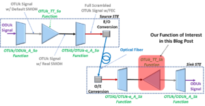
Figure 1, Illustration of Unidirectional Connection between a Source STE and a Sink STE with the OTUk_TT_Sk function highlighted.

Once this OTUk data arrives at the OTUk_TT_Sk function, it will perform the following tasks on this data stream.

Extracts and Processes the OTUk-SMOH within the incoming OTUk Data-Stream

The OTUk_TT_Sk function will accept this OTUk data stream and extract and process the OTUk-SMOH data from the incoming OTUk signal.  The OTUk_TT_Sk function will evaluate this data to check for various defects and errors.

In other words, the OTUk_TT_Sk function will evaluate the OTUk_SMOH (the OTUk_TT_So function, at the remote STE) created.  The OTUk_TT_Sk function will evaluate the OTUk-SMOH to check and see if it should declare certain types of defect conditions or if certain kinds of errors have occurred within this OTUk signal during transmission over optical fiber, as we describe below.

Clueless about OTN? We Can Help!!! Click on the Banner Below to Learn More!!!

Corporate Discounts Available!!

Detect and Flag Defects and Errors within the Incoming OTUk Data-Stream

More specifically, the OTUk_TT_So function will check the following defect conditions for (and declare or clear).

NOTE:  (*) – Indicates that you need to be a member of THE BEST DARN OTN TRAINING PRESENTATION…PERIOD!!!  to access this link.  

Additionally, the OTUk_TT_Sk function will also detect and flag the following errors (within this OTUk data stream):

Some Details about the OTUk_TT_Sk Function

Figure 2 presents a simple illustration of the OTUk_TT_Sk function.

OTUk_TT_Sk Function - Trail Trace Atomic Function

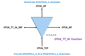
Figure 2, Simple Illustration of the OTUk_TT_Sk Atomic Function

The Interfaces within the OTUk_TT_Sk Atomic Function

Figure 2 shows that this function consists of four different interfaces.

  • OTUk_TCP – The OTUk Termination Connection Point:  This is where the function user supplies data (which most likely came from an upstream OTSi/OTUk-a_A_Sk or OTSiG/OTUk-a_A_Sk function) to the OTUk_TT_Sk function.  This data will typically consist of the entire OTUk data stream (without the FEC, which was already decoded by the upstream OTSi/OTUk-a_A_Sk or OTSiG/OTUk-a_A_Sk function).
  • OTUk_AP – The OTUk Access Point:  This is where the function outputs OTUk data, clock, frame, and multi-frame signals (of the incoming OTUk data-stream) to downstream circuitry (towards the OTUk/ODUk_A_Sk function).
  • OTUk_TT_Sk_MP – The Function Management Point:  This interface permits the function-user to exercise control and monitor the activity within the OTUk_TT_Sk function.  Some information the user can obtain from the Management Point includes Performance Monitoring and Correlated Defect Identification.
  • OTUk_TT_RP – The Function Remote Point:  This interface permits the function-user to output some information to a collocated OTUk_TT_So function.  This information includes the BDI, BEI, and BIAE indicators.  The collocated OTUk_TT_So function will respond to this signaling (from the OTUk_TT_Sk function – via the RP port) by transmitting the BEI values, BDI, and BIAE indicators back out to the Remote STE, as appropriate.

A Closer Look at the Interfaces within the OTUk_TT_Sk Function.

We will now take a closer look at these interfaces below.

The OTUk_TCP (Termination Connection Point) Interface

The OTUk_TT_Sk function accepts an OTUk data stream from either the upstream OTSi/OTUk-a_A_Sk or OTSiG/OTUk-a_A_Sk function via the OTUk_TCP Interface.

The data that either the OTSi/OTUk-a_A_Sk or the OTSiG/OTUk-a_A_Sk function outputs are a full-blown OTUk frame (that has been descrambled) by those functions.

Figure 3 presents a functional block of the OTUk_TT_Sk function.

OTUk_TT_Sk Functional Block Diagram

Figure 3, Functional Block Diagram of the OTUk_TT_Sk Function

Finally, Figure 3 shows that the equipment that we connect to the OTUk_TCP (of the OTUk_TT_Sk function) will supply the following signals to this function.

  • CI_D
  • CI_CK
  • CI_FS
  • CI_MFS

The OTUk_TT_Sk function will perform the following operations on each OTUk frame within this signal.

  • OTUk-SMOH (Section Monitoring Overhead) Extraction
  • Compute and Verify the BIP-8 Value
  • Receive and Process TTI (Trail-Trace Identifier) Messages
  • Declares and clears the following defects (as appropriate)
    • dIAE – Will also be forward to the RI_BIAE output in the form of the BIAE indicator.
    • dTIM  – Will be reported via the RI_BDI output by way of the BDI signal and will also be notified via the AI_TSF output.
    • dDEG – will also be reported via the AI_TSD output
    • dBDI
    • dBIAE

The OTUk_TT_Sk_MP (Management Point) Interface

As the OTUk_TT_Sk function performs all of the above actions on the data (that it receives via the OTUk_TCP Interface), it will tally and report all of the following performance monitoring parameters to System Management (via the Management Interface).

  • Report and Tally the following errors
    • BIP-8 Errors– reported as nBIPV (to the RI_REI output) and as nN_B in performance monitoring.
    • BEI Count – reported as nF_B in Performance Monitoring
  • To provide Performance Monitoring reports on the following parameters to System Management

Has Inflation got You Down? Our Price Discounts Can Help You Fight Inflation and Can Help You Become an Expert on OTN!! Click Below to Learn More!!

Discounts Available for a Short Time!!!

The OTUk_TT_Sk_RP (Remote Point) Interface

The OTUk_TT_Sk_RP Interface contains three (3) output ports that the System Designer should connect to the collocated OTUk_TT_So Atomic Function.

Whenever the user connects these three (3) output pins to similarly named pins at the collocated OTUk_TT_So function, these two functions will work together to transmit backward alarm and error information to the remote STE (the source of the OTUk data-stream that this OTUk_TT_Sk function is receiving).

Please click on the appropriate links to learn more about these backward (or far-end) indicators and how the OTUk_TT_Sk function accomplishes these forms of signaling with its collocated OTUk_TT_So function.

The OTUk_AP (Access Point) Interface (Output)

The OTUk_TT_Sk function will output the following signals via the OTUk_AP Interface.

  • AI_D – OTUk Adapted Information – Data Output
  • AI_CK – OTUk Adapted Information – Clock Output
  • AI_FS – OTUk Adapted Information – Frame Start Output
  • AI_MFS – OTUk Adapted Information – Multi-Frame Start Output
  • AI_TSF – OTUk Adapted Information – Trail Signal Fail (TSF) Indicator Output
  • AI_TSD – OTUk Adapted Information – Trail Signal Degrade (TSD) Indicator Output.

In most cases, the System Designer would route these output signals to the downstream OTUk/ODUk_A_Sk function for further processing.

AI_D, AI_CK, AI_FS, and AI_MFS will contain the remaining OTUk data-stream, clock, frame-start, and multi-frame start indicators for the OTUk/ODUk_A_Sk function.

Defect Notification – Downstream

The OTUk_TT_Sk function will assert the AI_TSF output pin anytime it declares a service-affecting defect (dTIM) itself or if the upstream circuitry (e.g., the OTSiG/OTUk-a_A_Sk or the OTSi/OTUk-a_A_Sk functions) are declaring service-affecting defects and asserting the CI_SSF input to this function.

Likewise, the OTUk_TT_Sk function will assert the AI_TSD output pin anytime it declares the dDEG (Signal Degrade) defect condition.

Consequent Actions

Consequent Action Equations specify what actions an Atomic Function should take any time (and for the duration) that it declares a certain defect.  ITU-T G.798 presents the following equations for consequent actions within the OTUk_TT_Sk function.

  • aTSF <- CI_SSF or [dTIM and (NOT TIMActDis)]
  • aBDI <- CI_SSF or dTIM
  • aBEI <- nBIPV
  • aBIAE <- dIAE
  • aTSD <- dDEG

I will discuss each of these consequent action equations below.

aTSF <- CI_SSF or [dTIM and (NOT TIMActDis)]

Where:  

aTSF is the Trail Signal Fail parameter that the OTUk_TT_Sk function will set LOW or HIGH to send current defect-state information towards downstream circuitry.

If aTSF = TRUE, then the OTUk_TT_Sk function will set its AI_TSF output HIGH.  Conversely, if aTSF = FALSE, then the OTUk_TT_Sk function will set its AI_TSF output to LOW.

CI_SSF is the current state of the CI_SSF (Server Signal Fail Indicator) input from the upstream OTSi/OTUk_A_Sk or OTSiG/OTUk_A_Sk atomic functions.  The OTSi/OTUk_A_Sk or OTSiG/OTUk_A_Sk function will assert this signal anytime it declares a service-affecting defect.

dTIM is the current state of the dTIM defect condition.

TIMActDis is a parameter the user can set to configure the dTIM to (optionally) drive the aTSF parameter.

This equation means that the OTUk_TT_Sk function will assert an internal signal (we call aTSF) if either of the following conditions is true.

  • The upstream circuitry (e.g., the OTSiG/OTUk-a_A_Sk or the OTSi/OTUk-a_A_Sk function) is asserting the CI_SSF input to this function, or
  • The OTUk_TT_Sk function declares the dTIM defect condition.

NOTES:

  1. If the OTUk_TT_Sk function asserts the aTSF signal, it will indicate so by asserting the AI_TSF output pin towards downstream circuitry (e.g., the OTUk/ODUk_A_Sk function).
  2. The AI_TSF output signal is a crucial signal for Automatic Protection Switching purposes.
  3. Please see the OTSi/OTUk_A_Sk or OTSiG/OTUk_A_Sk posts for information on what causes these two functions to drive the CI_SSF signal HIGH.

aBDI <- CI_SSF or dTIM

This equation means that the OTUk_TT_Sk function will assert another internal signal (the aBDI signal) if either of the following conditions is true.

  • The upstream circuitry (e.g., the OTSiG/OTUk-a_A_Sk or the OTSi/OTUk-a_A_Sk function) is asserting the CI_SSF input to this function, or
  • The OTUk_TT_Sk function declares the dTIM defect condition.

NOTES:

  1. If the OTUk_TT_Sk function asserts the aBDI signal, it will indicate so by asserting the RI_BDI output pin (via the Remote Point Interface).  This signaling will command the collocated OTUk_TT_So function to set its BDI bit-field to TRUE within its next outbound OTUk frame.
  2. The OTUk_TT_Sk function will assert the RI_BDI and AI_TSF output pins under the same conditions.
  3. Please see the OTSi/OTUk_A_Sk or OTSiG/OTUk_A_Sk posts for information on what causes these two functions to drive the CI_SSF signal HIGH.

aBEI <- nBIPV

This equation means that the OTUk_TT_Sk function will automatically set the internal signal aBEI to the total number of BIP-8 errors detected within a given OTUk frame.  This means the OTUk_TT_Sk function can set aBEI to a value between 0 and 8 within each OTUk frame.

NOTE:  If the OTUk_TT_Sk function sets aBEI to a particular value, it will set the RI_BEI output pin (via the Remote Point Interface) to this same value.  This signaling will command the collocated OTUk_TT_So function to set its BEI nibble-field to this same value (aBEI), within its next outbound OTUk frame, provided that RI_BIAE is set FALSE.

aBIAE <- dIAE

This equation means that the OTUk_TT_Sk function will assert the internal signal, aBIAE, if it declares the dIAE (Input Alignment Error) defect condition.

NOTES:

  1. If the OTUk_TT_Sk function is asserting the aBIAE signal, it will indicate so by asserting the RI_BIAE output pin (via the Remote Point Interface).  This signaling will command the collocated OTUk_TT_So function to set the BEI/BIAE nibble-field to reflect the BIAE condition within its next outbound OTUk frame.
  2. The OTUk_TT_Sk function will NOT assert the AI_TSF or RI_BDI output signals because it declares the dIAE defect condition.

aTSD <- dDEG

This equation means that the OTUk_TT_Sk function will assert the internal signal aTSD anytime it declares the OTUk-dDEG (Signal Degrade) defect condition.

NOTES:

  1.   If the OTUk_TT_Sk function is asserting the aTSD condition, it will indicate so by asserting the AI_TSD output signal towards the downstream circuitry (e.g., the OTUk/ODUk_A_Sk function in this case).
  2. The OTUk_TT_Sk function will NOT assert the RI_BDI output signal because it declares the dDEG defect condition.

The AI_TSD output signal is an essential signal for Automatic Protection Switching purposes.

The OTUk_TT_Sk Function Pin Description

Table 1 presents a Description of each of the Input and Output pins of the OTUk_TT_Sk function.

Table 1, Pin Description of the OTUk_TT_Sk Atomic Function

Signal NameTypeDescription
OTUk_TCP Interface
CI_DInputOTUk Characteristic Information - Data Input:
The OTUk_TT_Sk function will accept this data from either the upstream OTSi/OTUk-a_A_Sk or OTSiG/OTUk-a_A_Sk function via this input pin. The OTUk_TT_Sk function will then perform the following actions on this data.
- It will extract out and process the SMOH (Section Monitoring Overhead) and
-- Compute and Verify the BIP-8 data and it will detect and flag any BIP-8 errors within each OTUk frame.
-- It will extract out the Section Monitoring Byte and check the state of the BDI and IAE bit-fields.
-- It will read in the value of the BEI/BIAE nibble field and check for the BIAE indicator.
-- It will also read in and tally all non-zero (and non-BIAE) BEI values and BIP-8 errors.
-- It will extract out the TTI message and compare this read-out value with that of the expected TTI Message.

As the OTUk_TT_Sk performs all of these tasks it will declare or clear the following defect conditions (as warranted).
- dBDI
- dTIM
- dIAE
- dBIAE
- dDEG

It will tally the following events for Performance Monitoring purposes.
- pIAE - Number of seconds in which the OTUk_TT_Sk function declared the dIAE defect.
- pN_BIAE - Number of seconds in which the OTUk_TT_Sk function declared the dBIAE defect.
- pN_EBC - Number of Near-End Errored Block Counts (BIP-8 Errors).
- pN_DS - Number of Defect Seconds (seconds in which the OTUk_TT_Sk (or upstream circuitry) declared certain near-end defect conditions.
- pF_EBC - Number of Far-End Errored Block Counts (BEI Count)
- pF_DS - Number of Far-End Defect Seconds (seconds in which the OTUk_TT_Sk function is declaring the dBDI defect condition).

The OTUk_TT_Sk function will sample this data on one of the edges of the CI_CK input clock signal.
CI_CKInputOTUk Characteristic Information - Clock Input:
The OTUk_TCP Interface will use this clock input signal to sample all of the following input signals.
- CI_D
- CI_FS
- CI_MFS
- CI_SSF

This clock signal also functions as the timing source of the OTUk_TT_Sk function.
CI_FSInputOTUk Characteristic Information - Frame Start Input:
The upstream circuitry should drive this input signal HIGH whenever it is applying the very first bit/byte of a new OTUk frame to the CI_D input.

The upstream circuitry should drive this input signal HIGH once for each incoming OTUk frame.
CI_MFSInputOTUk Characteristic Information - Multi-Frame Start Input:
The upstream circuitry should drive this input signal HIGH whenever it is applying the very frist bit/byte of a new OTUk superframe to the CI_D input.

The upstream circuitry should drive this input signal HIGH once for each incoming OTUk superframe (or once every 256 OTUk frames).
CI_SSFInputOTUk Characteristic Information - Server Signal Failure Indicator Input:
This input pin indicates whether or not the upstream circuitry is declaring a service-affecting defect with the OTUk data-stream (that it is applying to the CI_D input). These service-affecting defects include:
- dLOF
- dLOM
- dAIS (for OTU1 or OTU2 applications only).

This signal is functionally equivalent to the AIS indicator.

LOW - Indicates that the upstream circuitry is NOT declaring a service-affecting defect with the OTUk signal (being applied to the CI_D input).

HIGH - Indicates that the upstream circuitry IS declaring a service-affecting defect with the OTUk signal (being applied to the CI_D input).
OTUk_AP Interface
AI_DOutputOTUk Adapted Information - Data Output:
The OTUk_TT_Sk function will output the OTUk data, after it has passed through and been processed by this function. This data will typicallly be routed to the OTUk/ODUk_A_Sk function for further processing.

This data will be updated (and output) synchronously with the AI_CK clock output signal.
AI_CK OutputOTUk Adapted Information - Clock Output:
The OTUk_TT_Sk function will update/output signals via the OTUk_AP Interface on one of the edges of this clock output signal.
- AI_D
- AI_FS
- AI_MFS
- AI_TSF
- AI_TSD
AI_FSOutputOTUk Adapted Information - Frame Start Output:
The OTUk_AP Interface will drive this output signal HIGH whenever it is also driving the very first bit/byte of a new OTUk frame via this AI_D output.

The OTUk_AP Interface will drive this output HIGH once for each outbound OTUk frame.
AI_MFSOutputOTUk Adapted Information - Multiframe Start Output:
The OTUk_AP Interface will drive this output signal HIGH whenever it is also driving the very first bit/byte of a new OTUk superframe via the AI_D output.

The OTUk_AP Interface will drive this output HIGH once for each oubound OTUk superframe.
AI_TSF OutputOTUk Adapted Information - Trail Signal Fail Output Indicator Output:
The OTUk_TT_Sk function will indicate whether or not it is declaring the Trail-Signal Fail (TSF) condition. The OTUk_TT_Sk function will declare the TSF condition, if it also declares any of the following defect conditions.
- dTIM
- SSF (if the CI_SSF input was driven HIGH due to any of the following defects within the upstream circuitry).
-- dLOF
-- dLOM
-- dAIS (OTU1/OTU2 applications only).

LOW - Indicates that the OTUk_TT_Sk function is NOT currently declaring the TSF indicator.

HIGH- Indicates that the OTUk_TT_Sk function is currently declaring the TSF indicator.
AI_TSDOutputOTUk Adapted Information - Trail Signal Declared Indicator Output:
The OTUk_TT_Sk function will use this output signal to indicate if it is declaring the Trail-Signal Defect (TSD) Condition. The OTUk_TT_Sk function will declare the TSD condition if it also declares the dDEG (Signal Degrade) defect condition.

LOW - Indicates that the OTUk_TT_Sk function is NOT currently declaring the TSD indicator.

HIGH - Indicates that the OTUk_TT_Sk function is currently declaring the TSD indicator.
OTUk_RP Interface
RI_BEIOutputOTUk Remote Point Information - Backward Error Indicator:
As the OTUk_TT_Sk function computes and verifies the BIP-8 values (within the OTUk signal that it is receiving via the CI_D input), it will output date through this output to reflect the number of BIP-8 errors that it is declaring within each incoming OTUk frame. This output signal will be connected to the RP input of its collocated OTUk_TT_So function.

If the OTUk_TT_Sk detects ZERO BIP-8 errors within the most recently received OTUk frame, then it will set RI_BEI = 0 for that OTUk frame period.

Likewise, if the OTUk_TT_Sk function detects five (5) BIP-8 errors within the most recenlty received OTUk frame, then it will set RI_BEI = 5 for that OTUk frame period.
RI_BIAEOutputOTUk Remote Point Information - Backward Input Alignment Error Indicator:
If the OTUk_TT_Sk function declares the dIAE defect condition, then it will set the RI_BIAE indicator true. This output signal will be connected to the corresponding RP Input of the collocated OTUk_TT_So function.

The collocated OTUk_TT_So function is expected to overwrite the BEI nibble-field (within the next outbound OTUk frame).

Please see the OTUk_TT_So function post for more details on this topic).
RI_BDIOutputOTUk Remote Point Information - Backward Defect Indicator:
If the OTUk_TT_Sk function declares any of the following defect conditions, then it will set this output pin TRUE.
- dTIM
- CI_SSF

The user should connect this output signal to the RI_BDI input of the collocated OTUk_TT_So function.

The collocated OTUk_TT_So function is expected to set the BDI bit-field (within the Section Monitoring byte of the SMOH) to "1" within the next outbound OTUk frame, if this output pin is TRUE.

Otherwise, the OTUk_TT_So function should set the BDI bit-field to "0" within the very next outbound OTUk frame.
OTUk_TT_So_MP Interface
MI_AcTIOutputManagement Interface - Accepted Trail Trace identifier Message Output:
The OTUk_TT_Sk function will output the contents of the Accepted Trail Trace Identifier Message via this output signal.

The OTUk_TT_Sk function will output the accepted TTI Message via this output, whenever the user issues a command requesting this data via the MI_GetAcTI input.
MI_ExSAPIInputManagement Interface - Expected SAPI (Source Access Point Identifier) Input:

The OTUk_TT_Sk function will compare the SAPI-portion of the "Accepted Trail-Trace Identification" Message (that it receives from the SMOH (within the OTUk signal) with that which the user supplies to this input.

If the two values do not match, then the OTUk_TT_Sk function will declare the dTIM defect condition.
MI_ExDAPIInputManagement Interface - Expected DAPI (Destination Access Point Identifier) Input:
The function user is expected to apply the Expected Value of the DAPI portion of the Trail-Trace Identification Message.

The OTUk_TT_Sk function will compare the DAPI portion of the "Accepted Trail-Trace Identification" Message (that it received from the SMOH (within the OTUk signal) with that which the user supplies to this input.

If the two values do not match, then the OTUk_TT_Sk function will declare the dTIM defect condition.
MI_GetAcTIInputMangement Interface - Get Accepted Message Command Input:
This input permits the user to request that the OTUk_TT_Sk function provide the user with the currently "accepted" TTI Message. Whenever the user invokes this command, the OTUk_TT_Sk function will output the contents of the currently "accepted" TTI Message via the MI_ActTI output.
MI_TIMDetMoInputManagement Interface - TIM (Trace Identifier Mismatch) Detection Mode:
This input permits the user to specify which portion of the TTI Message that the OTUk_TT_Sk function should check and verify when checking for the dTIM defect condition. Please see the dTIM blog post for more details.
MI_cTIMOutputManagement Interface - Correlated TIM (Trail-Trace Identifier Mismatch) Defect:
This output signal indicates if the OTUk_TT_Sk function is declaring the dTIM defect condition.

LOW - Indicates that the OTUk_TT_Sk function is NOT currently declaring the dTIM defect condition.

HIGH - Indicates that the OTUk_TT_Sk function is currently declaring the dTIM defect condition.
MI_cDEGOutputManagement Interface - Correlated DEG (Signal Degrade) Defect:
This output signal indicates if the OTUk_TT_Sk function is declaring the dDEG defect condition.

LOW - Indicates that the OTUk_TT_Sk function is NOT currently declaring the dDEG defect condition.

HIGH - Indicates that the OTUk_TT_Sk function is currently declaring the dDEG defect condition.
MI_cBDIOutputManagement Interface - Correlated BDI (Backward Defect Indicator) Defect:
This output signal indicates if the OTUk_TT_Sk function is declaring the dBDI defect condition.

LOW - Indicates that the OTUk_TT_Sk function is NOT currently declaring the dBDI defect condition.

HIGH - Indicates that the OTUk_TT_Sk function is currently declaring the dBDI defect condition.
MI_cSSFOutputManagement Interface - Correlated SSF (Server Signal Fail) Defect:
This output signal indicates if the OTUk_TT_Sk function is declaring the SSF defect condition.

LOW - Indicates that the OTUk_TT_Sk function is NOT currently declaring the SSF defect condition. This also means that the upstream circuitry is currently drving the CI_SSF input pin LOW.

HIGH - Indicates that the OTUk_TT_Sk function is currently declaring the SSF defect condition. This also means that upstream circuitry is currently driving the CI_SSF input pin HIGH.
MI_pIAEOutputManagement Interface - IAE Performance Monitor Parameter:
The OTUk_TT_Sk function will drive this output pin HIGH, for one full second, if it has declared the dIAE defect for any portion of the previouis one-second period.

Conversely, the function will keep this output pin LOW, for one full second, if it has NEVER declared the dIAE defect, during the previous one-second period.

This one second period will be dictated by the 1-Second Clock signal that the user supplies to the MI_1Second input to this function.
MI_pBIAEOutputManagement Interface - BIAE Performance Monitor Parameter:
The OTUk_TT_Sk function will drive this output pin HIGH for one full second, if it has declared the dBIAE defect for any portion of the previous one second period.

Conversely, the function will keep tis output pin LOW for one full second, if it has NEVER declared the dBIAE defect, during the previous one second period.

This one second period will be dictated by the 1 Second Clock signal that the user supplies to the MI_1Second input to this function.
MI_pN_EBCOutputManagement Interface - Number of Near-End Errored Block Count (BIP-8 Errors) - One Second Performance Monitoring Parameter:
The OTUk_TT_Sk function will tally and report the total number of BIP-8 errors, that it has detected and flagged (within the incoming OTUk data-stream), during the previous 1 second period.
MI_pN_DSOutputManagement Interface - Near-End Defect - One Second Performance Monitoring Parameter:
The OTUk_TT_Sk fuinction will drive this output pin HIGH for one full second, if it has declared at least one of the following defects for any portion of the previous one-second period.
- CI_SSF or
- dTIM

Conversely, the function will keep this output pin LOW, for one-full second, if it has NEVER declared any of these defect during the previous one-second period.

This one-second period will be dictated by the 1 Second Clock signal that the user supplies to the MI_1Second input to this function.
MI_pF_EBCOutputManagement Interface - Number of Far-End Errored Block Count (BEI Errors) - One Second Performance Monitoring Parameter:
The OTUk_TT_Sk function will tally and report the total number of BEI counts that it has read and captured (within the incoming OTUk data-stream) during the previous one-second period.
MI_pF_DSOutputManagement Interface - Far-End Defect - One Second Performance Monitoring Parameter:
The OTUk_TT_Sk function will drive this output pin HIGH, for one full second, if it has declared the dBDI defect for any portion of the previous one-second period.

Conversely, this function will keep this output pin LOW, for one-full second, if it has NEVER declared the dBDI defect, during the previous one-second period.
MI_1SecondInputManagement Interface - One Second Clock Input:
The user is expected to supply a clock signal, which has a frequency of 1Hz, to this input.

The Performance Monitoring portino of the OTUk_TT_Sk function will use this clock signal as its timing reference for tallying and reporting the various one-second Performance Monitoring parameters.
MI_DEGThrInputManagement Interface - The dDEG BIP-8 Error Threshold for a Bad One-Second Interval:
The user can specify the BIP-8 error threshold for which the OTUk_TT_Sk function should count a given one second period as a "Bad One-Second" period, for the sake of dDEG declaration.

If the OTUk_TT_Sk function detects DEGThr or more BIP-8 errors, during a one-second interval, then the OTUk_TT_Sk function will count that one-second interval as a "Bad" interval.

If the OTUk_TT_Sk function detects less than DEGThr BIP-8 errors, during a one-second interval, then the OTUk_TT_Sk function will NOT count that one-second as a "Bad" interval.
MI_DEGMInputManagement Interface - Number of "Bad One-Second" Intervals for dDEG Declaration:
The user can specify the minimum number of consecutive "Bad One Second" intervals that the OTUk_TT_Sk function must detect before declaring the dDEG defect condition.

If the OTUk_TT_Sk function detects and flags DEGM consecutive "Bad One-Second" Intervals, then the OTUk_TT_Sk function will declare the dDEG defect condition.

NOTE: DEGThr defines the threshold for a "Bad One-Second" interval.

Has Inflation got You Down? Our Price Discounts Can Help You Fight Inflation and Help You to Become an Expert on OTN!! Click on the Banner Below to Learn More!!

Discounts Available for a Short Time!!

For More Information on OTN Posts in this Blog, click on the Image below.

OTN Related Blog

OTN Related Topics within this Blog

OTN Related Topics within this Blog General Topics Consequent Equations - What are they and How can you use them? ...

What is the OTUk/ODUk_A_Sk Atomic Function?

This post briefly describes the OTUk/ODUk_A_Sk Atomic Function. The OTUk/ODUk_A_Sk function is also known as the OTUk to ODUk Adaptation Sink Function. This function will take an OTUk signal and it will extract/de-map out the ODUk signal within.


What is the OTUk/ODUk_A_Sk Atomic Function?

We formally call the OTUk/ODUk_A_Sk Atomic Function the OTUk to ODUk Adaptation Sink Function.

Introduction

The OTUk/ODUk_A_Sk function performs the exact reverse operation, as does the OTUk/ODUk_A_So function.

NOTE:  We extensively discuss the OTUk/ODUk_A_Sk function within Lesson 9 of THE BEST DARN OTN TRAINING PRESENTATION…PERIOD!!!

More specifically, this function will:

  • Accept an OTUk signal (from upstream circuitry) and
  • Extract (or de-map) out an ODUk signal from this signal.

Figure 1 presents a simple illustration of the OTUk/ODUk_A_Sk function.

OTUk/ODUk_A_Sk Function - Adaptation Atomic Function

Figure 1, Simple Illustration of the OTUk/ODUk_A_Sk Function

As the OTUk/ODUk_A_Sk function converts an OTUk signal into an ODUk signal, it will terminate, process, and remove the OTUk-SMOH from this incoming OTUk data stream.  It will also extract the ODUk signal from this OTUk signal and route it to the downstream ODUk circuitry for further processing.

Please see the post on the ODUk_TT_Sk atomic function for more information on how ITU-T G.798 recommends that we handle and process ODUk signals.

The Interfaces within the OTUk/ODUk_A_Sk Function

Figure 1 shows that this function consists of the following three interfaces.

  • OTUk_AP – The OTUk Access Point:  This is the interface where the function user supplies the OTUk data to the function.  The upstream OTUk_TT_Sk function usually drives the signals within this interface.
  • ODUk_CP – The ODUk Connection Point:  This is where the function outputs ODUk data, clock, frame, and multi-frame signals (of the extracted ODUk data-stream) towards the ODUk-client circuitry.
  • OTUk/ODUk_A_So_MP – The Function Management Point:  This interface permits the function user to exercise control and monitor the activity within the OTUk/ODUk_A_Sk function.  This interface also allows the ODUk-client to access the APS channel (within the ODUk data stream).

Functional Block Diagram

Figure 2 presents the functional block diagram of the OTUk/ODUk_A_Sk function.

OTUk/ODUk_A_Sk Atomic Functional Block Diagram

Figure 2, Functional Block Diagram of the OTUk/ODUk_A_Sk Function

This figure shows the upstream equipment (e.g., the OTUk_TT_Sk function), which we typically connect to the OTUk_AP Interface (of the OTUk/ODUk_A_Sk function), will supply the following signals to this function.

  • AI_D – OTUk data (with the SMOH)
  • AI_CK – The OTUk clock input signal
  • AI_FS – The OTUk Frame Start Input signal
  • AI_MFS – The OTUk Multi-frame Start Input signal

Clueless about OTN? We Can Help!!! Click on the Banner Below to Learn More!!!

Corporate Discounts Available!!

So What All Does this Atomic Function Do?

The OTUk/ODUk_A_Sk function will perform the following operations on these signals.

It will extract out/de-map the ODUk Data-Stream, the De-Mapping (ODUk) Clock Signal (ODCr), and it will generate the FS (Frame Start) and MFS (Multi-Frame Start) Signals.

The OTUk/ODUk_A_Sk function will de-map out and generate the following signals from the incoming OTUk signal.

  • ODUk Data-Stream – The ODUk Data consists of both the ODUk Overhead (PMOH) and the ODUk payload data
  • The ODUk Clock – The ODUk Clock Output signal
  • ODUk FS – The ODUk Frame Start Output
  • ODUk MFS – The ODUk Multi-frame Start Output

Extract out APS (Automatic Protection Switching) Commands from the APS Channel (within the ODUk-PMOH)

Once the OTUk/ODUk_A_Sk function has extracted the ODUk Data (which consists of the ODUk Overhead and Payload data), this function will now give the user access to the APS Channel (which is available via the APS/PCC field within the ODUk Overhead).

This function will route the APS Command information (within APS/PCC Channel) to the CI_APS output.

Transmits Either a Normal ODUk signal or the ODUk-LCK or ODUk-AIS Maintenance Signals downstream

The user can configure the OTUk/ODUk_A_Sk function to either output Normal (an ODUk signal carrying client-information) data or the ODUk-LCK maintenance signal, depending upon what the user does with the MI_AdminState input (to this function).

The user can also configure this function to automatically generate the ODUk-AIS Maintenance signal (instead of the NORMAL signal) whenever upstream circuitry asserts the AI_TSF input (to this function).

Function Defects

The OTUk/ODUk_A_Sk function does not internally declare any defects.

Consequent Actions

ITU-T G.798 presents the following equations for consequent actions within this particular function.

  • aSSF <- AI_TSF and (NOT MI_AdminState = LOCKED)
  • aAIS <- AI_TSF and (NOT MI_AdminState = LOCKED)
  • aSSD <- AI_TSD and (NOT MI_AdminState = LOCKED)

I will discuss each of these consequent action equations below.

aSSF <- AI_TSF and (NOT MI_AdminState = LOCKED)

This equation means two things.

  • The function will NOT declare the SSF (Server Signal Failure) condition if the user configures the MI_AdminState input into the LOCKED position.
  • The function will declare the SSF condition if the upstream OTUk_TT_Sk function drives the AI_TSF input pin TRUE (and if the user has NOT set the MI_AdminState to the LOCKED position).

NOTE:  If the OTUk/ODUk_A_Sk function declares the SSF condition, it will indicate so by asserting the CI_SSF output pin towards downstream circuitry.

The CI_SSF output signal is a crucial signal for Automatic Protection Switching purposes.

aAIS <- AI_TSF and (NOT MI_AdminState = LOCKED)

This equation means two things.

  • Suppose the user sets the MI_AdminState input to the LOCKED position.  In that case, this function will unconditionally generate and transmit the ODUk-LCK Maintenance Signal (via the CI_D output), regardless of the current state of the AI_TSF input to this function.
  • The OTUk/ODUk_A_Sk function will automatically generate and transmit the ODUk-AIS Maintenance Signal (via the CI_D output signal of this function) if the AI_TSF input pin is set to TRUE (provided that the MI_AdminState input is NOT set to the LOCKED position).

This equation also means that this function will only transmit a NORMAL ODUk signal (carrying client data) if the MI_AdminState input is NOT in the LOCKED position and the AI_TSF input pin is set FALSE.

aSSD <- AI_TSD and (NOT MI_AdminState = LOCKED)

This equation means two things.

  • This function will not declare the SSD (Server Signal Degrade) condition if the user configures the MI_AdminState input into the LOCKED position.
  • The function will declare the SSD condition if the upstream OTUk_TT_Sk function drives the AI_TSD input pin TRUE (and if the user has NOT set the MI_AdminState to the LOCKED position).

NOTE:  If the OTUk/ODUk_A_Sk function declares the SSD condition, it will indicate so by asserting the CI_SSD output pin towards downstream circuitry.

The CI_SSD output signal is a crucial signal for Automatic Protection Switching purposes.

How do the AI_TSF and MI_AdminState input signals affect the CI_SSF and CI_D outputs (from this function)?

The Consequent Equations for aSSF and aAIS all show that the function outputs (via the CI_SSF and CI_D pins) depend upon the state of the AI_TSF and MI_AdminState Inputs, as we offer in Table 1 below.

Table 1, Truth Table of the CI_D and CI_SSF Output Signals, based upon the AI_TSF and MI_AdminState Inputs

Relationship between AI_TSF and MI_AdminState inputs and CI_SSF and CI_D Outputs - OTUk/ODUk_A_Sk Function

Defect Correlations

None for this function.

Performance Monitoring

None

Pin Description

Table 2 presents a list and description of each input and output signal for the OTUk/ODUk_A_Sk function.

Table 2, List and Definition for each Input and Output Signal in the OTUk/ODUk_A_Sk function

Signal NameTypeDescription
OTUk_AP Interface
AI_DInputOTUk Adapted Information - OTUk Input:
The upstream OTUk_TT_Sk function is expected to apply a bare-bones OTUk data-stream to this input.

NOTE: This OTUk data will contain the following fields:
- OTUk SMOH data
- The contents of the APS/PCC channel (within the ODUk Overhead) and
- The rest of the OTUk frame.

This OTUk data-stream will not include the FAS, MFAS or FEC fields
AI_CKInputOTUk Adapted Information - Clock Input
This clock signal will sample all data that the user supplies to the AI_D, AI_FS, AI_MFS, AI_TSF and AI_TSD inputs.

The OTUk/ODUk_A_Sk function will also use this clock signal as its base timing source.
AI_FSInputOTUk Adapted Information - Frame Start Input:
The upstream OTUk_TT_Sk function will drive this signal TRUE; coincident to whenever it is supplying the very first bit or byte (of a given OTUk frame) to the AI_D input.

The upstream OTUk_TT_Sk function is expected to assert this signal once for each OTUk frame period.
AI_MFSInputOTUk Adapted Information - Multiframe Start Input:
The upstream OTUk_TT_Sk function will drive this signal TRUE coincident to whenever it is supplying the very first bit or byte (of a given OTUk Superframe) to the AI_D input.

The upstream OTUk_TT_Sk function is expected to assert this signal once for each OTUk superframe period, or once every 256 OTUk frame periods.
AI_TSFInputOTUk Adapted Information - Trail Signal Fail Indicator
The upsteam equipment (e.g., the OTUk_TT_Sk function) will typically assert this input pin whenever it is declaring one (or more) service-affecting defects wit the data that it is ultimately applying to the AI_D input of this function.

This signal has a similar role to the AIS signal. Please see the blog post on AIS for more information on this topic.
AI_TSDInputOTUk Adapted Information - Trail Signal Degrade Indicator Input:
The upstream equipment (e.g., the OTUk_TT_Sk function) will typically assert this input whenever it is declaring the dDEG (Signal Degrade) defect with the data that it is ultimately applying to the AI_D input of this function.
ODUk_CP Interface
CI_DOutputODUk Characteristic Information - ODUk Data Output:
The OTUk/ODUk_A_Sk function will take the ODUk data (that it has de-mapped from the OTUk signal, applied at the AI_D input) and output this data via this output signal.

However, if the user commands this function to output the ODUk-LCK Maintenance Signal, then it will do so via this output pin.

Finally, this function will also output the ODUk-AIS Maintenance Signal via this output if conditions warrant.
CI_CKOutputODUk Characteristic Information - Clock Output:
As the ODUk_CP Interface outputs data via the CI_D, CI_FS, CI_MFS, CI_APS, CI_SSF and CI_SSD outputs, all of this data will be updated on one of the clock edges of this clock output signal.
CI_FSOutputODUk Characteristic Information - Frame Start Output:
The ODUk_CP interface will pulse this output signal HIGH whenever the ODUk_CP interface outputs the very first bit (or byte) of a new ODUk frame, via the CI_D output.

This output signal will pulse HIGH once for each ODUk frame.
CI_MFSOutputODUk Characteristic Information - Multiframe Start Output:
The ODUk_CP Interface will pulse this output signal HIGH whenever the ODUk_CP interface outputs the very first bit (or byte) of a new ODUk Superframe, via the CI_D output.

This output signal will pulse HIGH once for each ODUk Superframe (or once each 256 ODUk frames).
CI_SSFOutputODUk Characteristic Information - Server Signal Failure Indicator Output:
One can think of this output pin as a buffered version of the AI_TSF input pin. This function will drive this output pin HIGH anytime the AI_TSF input pin (at the OTUk_AP Interface) is driven HIGH.

Conversely, this function will drive this output pin LOW anytime the AI_TSD input pin is driven LOW.
CI_SSDOutputODUk Characteristic Information - Server Signal Degrade Output:
One can think of this output pin as a buffered version of the AI_TSD output pin. This function will drive this output pin HIGH anytime the AI_TSD input pin (at the OTUk_AP Interface) is driven HIGH.

Conversely, this function will drive this output pin LOW anytime the AI_TSD input pin is driven LOW.
CI_APSOutputODUk Characteristic Information - APS Channel Output:
The OTUk/ODUk_A_Sk function will extract out the contents of the APS channel (from the incoming ODUk data-stream) and it will output the contents of the APS/PCC channel (as it applies to the APS Level that this OTUk/ODUk_A_Sk function is operating at).
OTUk/ODUk_A_Sk_MP Interface
MI_AdminStateInputManagement Interface - AdminState Input:
This input permits the function user to configure the OTUk/ODUk_A_Sk function to output either NORMAL ODUk data, or the ODUk-LCK maintenance signal via the CI_D output of this function.

Setting this input pin to the LOCKED state will configure the OTUk/ODUk_A_Sk function to override the NORMAL ODUk data, and the ODUk-AIS maintenance signal with the ODUk-LCK maintenance signal.
MI_APS_EnInputManagement Interface - APS Enable Input
This input permits the function user to either enable or disable APS/PCC Channel extraction from the incoming ODUk data-stream.

Setting this input pin TRUE configures the OTUk/ODUk_A_Sk function to extract the APS Messages from the APS/PCC channel (within the ODUk Overhead of the incoming ODUk data-stream) and output this data via the CI_APS output port.

Conversely, setting this input pin FALSE disables APS Message extraction from the incoming ODUk data-stream.
MI_APS_LVLInputManagement Interface - APS Level Input:
This input permits the user to specify the APS Level for this instantiation of the OTUk/ODUk_A_Sk function.

If the MI_APS_En input is TRUE, then this input pin will select the APS Level (and that portion of the APS/PCC Channel) that this function will output via the CI_APS output. Please see the APS/PCC post on more information about this protocol.

If the MI_APS_En input is FALSE, then this input will be ignored.

Has Inflation got You Down? Our Price Discount Can Help You Fight Inflation and Help You Become an Expert on OTN!! Click on the Banner Below to Learn More!!

Discounts Available for a Short Time!!!

For More Information on OTN Posts in this Blog, click on the Image below.

OTN Related Blog

OTN Related Topics within this Blog

OTN Related Topics within this Blog General Topics Consequent Equations - What are they and How can you use them? ...

What is the OTUk/ODUk_A_So Atomic Function?

This post briefly describes the OTUk/ODUk_A_So (OTUk to ODUk Adaptation Source) Function. This function will take an ODUk signal and it will synchronously map it into an OTUk signal.


What is the OTUk/ODUk_A_So Atomic Function?

We formally call the OTUk/ODUk_A_So Atomic Function the OTUk to ODUk Adaptation Source Function.

Introduction

The OTUk/ODUk_A_So function is any circuit that (1) accepts an ODUk signal and (2) adapts (or maps) it into an OTUk signal for transmission to the following Trail Termination Function.

NOTE:  If we are working with a Fully-Compliant OTUk frame, then the OTUk/ODUk_A_So function will synchronously map each ODUk frame into the OTUk frame.

On the other hand, if we are working with a Functionally-Compliant OTUkV frame, this mapping might be asynchronous.

In this post, we will assume that we are working with a Fully-Compliant OTUk frame.

NOTE:  We discuss the OTUk/ODUk_A_So function in detail in Lesson 9, within THE BEST DARN OTN TRAINING PRESENTATION…PERIOD!!!

Figure 1 presents a simple illustration of the OTUk/ODUk_A_So function.

OTUk/ODUk_A_So Simple Block Diagram - ITU-T G.798 Symbol

Figure 1, Simple Illustration of the OTUk/ODUk_A_So function

As the OTUk/ODUk_A_So function converts an ODUk signal into an OTUk signal, it will encapsulate each ODUk frame into an OTUk frame by adding the OTUk Overhead to the ODUk structure.

Please note that the OTUk/ODUk_A_So function will only insert default values for the SMOH (Section Monitoring Overhead) within the OTUk overhead.

Functional Block Diagram for the OTUk/ODUk_A_So Function

Figure 2 presents a Functional Block Diagram for the OTUk/ODUk_A_So function.

OTUk/ODUk_A_So Functional Block Diagram

Figure 2, Functional Block Diagram for the OTUk/ODUk_A_So function

Interfaces within the OTUk/ODUk_A_So Function

Figure 2 shows that this function consists of three different interfaces.

  • ODUk_CP – The ODUk Connection Point.  The ODUk_CP is the interface where the ODUk-client supplies ODUk characteristic information (CI) to the OTUk/ODUk_A_So function input.
  • OTUk_AP – The OTUk Access Point.  There is where the OTUk/ODUk_A_So function outputs OTUk data, clock, frame, and multi-frame signals (for the outbound OTUk data-stream) to downstream circuitry (towards the OTUk_TT_So function).
  • OTUk/ODUk_So_MP – The Function Management Point.  This interface permits the function user to exercise control of the activity within the OTUk/ODUk_A_So function.

Figure 2 shows that the ODUk-client function (connected to the ODUk_CP Interface – of the OTUk/ODUk_A_So function) will supply the following signals to this function.

  • CI_D – ODUk Data-Stream
  • CI_CK – ODUk Clock Signal
  • CI_FS – ODUk Frame Start Signal
  • CI_MFS – ODUk Multiframe Start Signal
  • CI_APS – ODUk APS Communication Channel

Clueless about OTN? We Can Help!!! Click on the Banner Below to Learn More!!!

Corporate Discounts Available!!

So What Does This Function Do?

The OTUk/ODUk_A_So function will perform the following operations on these signals.

Optionally Generates the ODUk-LCK Maintenance Signal

The function allows the user to configure the OTUk/ODUk_A_So function to generate the ODUk-LCK maintenance signal upon command internally.

The user can implement this command by setting the MI_AdminState input pin (at the Management Port) into the LOCKED State.

Whenever the user sets the MI_AdminState input into the LOCKED State and commands the OTUk/ODUk_A_So function to generate the ODUk-LCK maintenance signal, the timing, framing, and multi-framing for this ODUk-LCK signal will be based on the CI_CK, CI_FS and CI_MFS inputs (at the ODUk_CP Interface).

NOTE:  In this case, the ODUk-LCK maintenance signal will replace the ODUk traffic carrying user/client data.

This function will, in turn, map this replacement signal into an OTUk data stream. 

Please see the post on the ODUk-LCK maintenance signal for more details about the ODUk-LCK maintenance signal.

Allows User to Insert APS (Automatic Protection Switching) Commands into the APS Channel (within the ODUk-PMOH).

The OTUk/ODUk_A_So function permits the user to access the APS channel (within this ODUk signal) via some inputs (at both the OTUk/ODUk_A_So_MP and the ODUk_CP Interfaces).

More specifically, this function allows the user to enable or disable the APS Channel and configure this function to operate at a specific APS Level through the MI_APS_En and MI_APS_LVL inputs (via the OTUk/ODUk_A_So_MP Interface).

Additionally, this function permits the user to insert their own APS Commands into the APS/PCC Channel within the ODUk Overhead via the CI_APS input (at the ODUk_CP Interface).

NOTE:  Please see the relevant post on the APS/PCC Channel to learn more about the APS Channel.

Generates OTUk Clock, FS (Frame Start), and MFS (Multi-Frame Start) Signals via the OTUk_AP Interface

The OTUk/ODUk_A_So function will synthesize the clock (AI_CK), frame start (AI_FS), and multi-frame start (AI_MFS) signals for the outbound OTUk signal via the OTUk_AP Interface.

The OTSiG/OTUk_A_So or OTSi/OTUk_A_So function (downstream) will use these signals to generate and insert the FAS and MFAS fields into the correct locations within the outbound OTUk data stream.

Generates the IAE (Input Alignment Error) Indicator for the downstream OTUk_TT_So function

The OTUk/ODUk_A_So function will generate the IAE (Input Alignment Error) indicator anytime it detects a frame-slip within the incoming ODUk signal (e.g., CI_FS) via the ODUk_CP Interface.

In other words, if this function detects the CI_FS signal pulsing TRUE during an unexpected clock cycle (CI_CK), then this function will drive the AI_IAE output pin HIGH

Whenever the OTUk/ODUk_A_So function drives the AI_IAE output pin HIGH, it signals an Input Alignment Error Event.   The OTUk/ODUk_A_So function will drive the AI_IAE output signal to the downstream OTUk_TT_So function.  

The downstream OTUk_TT_So function will accept and perform another process with this AI_IAE output signal.

The OTUk/ODUk_A_So function will keep the AI_IAE output pin HIGH until the upstream (ODUk-circuitry) starts to assert the  CI_FS input indicator during the correct (or expected) CI_CK period, once again.

Generate and Route the OTUk Data-Stream to downstream circuitry

This function will output a data stream via the AI_D output, which I will call a partial OTUk data stream

This data stream will not contain the FAS, MFAS, or the FEC fields. 

It will include the ODUk-portion of the OTUk frame and the default values for the various OTUk Overhead Fields (e.g., the Section Monitoring Overhead – SMOH).

We will then route this data stream to other circuitry (e.g., the OTUk_TT_So function) for further processing.

List of Input and Output Signals for the OTUk/ODUk_A_So Function

Table 1 presents a list and description for each OTUk/ODUk_A_So function input and output ports.

Table 1, List and Definition for each Input and Output Signal in the OTUk/ODUk_A_So function

Signal NameTypeDescription
ODUk_CP Interface
CI_DInputODUk Characteristic Information - Data Input:
The ODUk-client is expected to input the ODUk data via this input. This ODUk data will contain all portions of the ODUk frame.
CI_CKInputODUk Characteristic Information - Clock Input:
This clock signal will sample all data that the ODUk-client supplies to the CI_D, CI_FS, CI_MFS and CI_APS inputs.

The OTUk/ODUk_A_So function will also use this clock signal as its timing source.
CI_FSInputODUk Characteristic Information - Frame Start Input:
The ODUk-client equipment will drive this signal TRUE; coincident to whenever it is supplying the very first bit or byte (of a given OTUk frame) to the CI_D input.

The ODUk-client is expected to assert this signal once for each ODUk frame period.

The OTUk/ODUk_A_So function will also use this input signal to determine if it should declare the IAE condition, via the AI_IAE output pin.
CI_MFSInputODUk Characteristic Information - Multiframe Start Input:
The system-side equipment will drive this signal TRUE coincident to whenever it is supplying the very first bit or byte (of a given ODUk/OTUk Superframe) to the CI_D input.

The ODUk-client is expected to assert this signal once for each OTUk/ODUk superframe period, or once every 256 ODUk frame periods.
CI_APSInputODUk Characteristic Information - APS Channel Data:
The system-side equipment is expected to apply the APS Channel to this input.

The function user must set the MI_APS_En input to TRUE and must place a valid value (for APS Level) at the MI_APS_LVL input pins, or the OTUk/ODUk_A_So function will ignore the data at this input.

The OTUk/ODUk_A_So function will map this data into the APS/PCC channel within the ODUk data-stream.

Please see the blog post about the APS/PCC channel for more information.
OTUk_AP Interface
AI_DOutputOTUk Adapted Information - OTUk Data Output:
The OTUk/ODUk_A_So function will take all of the data (that the ODUk-client applies to both the CI_D and CI_APS input pin) and will combine this data together to form a bare-bones OTUk data-stream.

NOTE: This OTUk data will contain the following fields.
- Default OTUk SMOH data,
- The contents of the APS/PCC channel and
- The rest of the OTUk frame.

This OTUk data-stream will not include the FAS, MFAS or FEC fields. Additionally, the downstream OTUk_TT_So function will compute and generate the correct values for the OTUk-SMOH.
AI_CKOutputOTUk Adapted Information - Clock Output:
As the OTUk_AP Interface outputs data via the AI_D, AI_FS, AI_MFS and AI_IAE outputs; it will updata all of this data on one of the edges of this clock output signal.
AI_FSOutputOTUk Adapted Information - Frame Start Output:
The OTUk_AP Interface will pulse this output signal HIGH whenever the OTUk_AP Interface outputs the very first bit (or byte) of a new OTUk frame, via the AI_D output.

The OTUk_AP Interface will pulse this output HIGH once for each outbound OTUk frame.
AI_MFSOutputOTUk Adapted Information - Multiframe Start Output:
The OTUk_AP Interface will pulse this output signal HIGH whenever the OTUk_AP Interface outputs the very first bit (or byte) of a new OTUk superframe, via the AI_D output.

The OTUk_AP Interface will pulse this output HIGH once for each OTUk Superframe (or once each 256 OTUk frames).
AI_IAEOutputOTUk Adapted Information - Input Alignment Error Output:
The OTUk_AP Interface will drive this output signal HIGH whenever the OTUk/ODUk_A_So function detects a frame slip within the ODUk_CP Interface.

More specifically, if the OTUk/ODUk_A_So determines that the upstream equipment has pulses the CI_FS input at an unexpected CI_CK period, then this function will drive this output HIGH.

This function will keep this output signal HIGH until the OTUk/ODUk_A_So function starts to receive pulses at the CI_FS during the "expected" CI_CK periods again.

Once the OTUk/ODUk_A_So function starts to receive pulses at the CI_FS input (during the "expected" CI_CK period) then it will drive this output pin LOW.
OTUk/ODUk_A_So_MP Interface
MI_AdminStateInputManagement Interface - AdminState Input:
This input pin permits the user to configure the OTUk/ODUk_A_So function to operate in either the LOCKED State or the NORMAL state.

If the user configures this function to operate in the NORMAL state, then it will map NORMAL ODUk traffic (e.g., ODUk traffic that is carrying client-data) into an OTUk frame as it passes through this function.

Conversely, if the user configures this function to operate in the LOCKED state, then the function will generate and map the ODUk-LCK Maintenance signal into the outbound OTUk data-stream.
MI_APS_EnInputManagement Interface - APS Channel Enable Input:
This input pin permits the user to either enable or disable the OTUk/ODUk_A_So function to/from accessing the APS/PCC channel within the ODUk overhead.

Setting this input HIGH permits the OTUk/ODUk_A_So function to access (and send APS messages via) the APS/PCC channel.

Setting this input LOW prevents the OTUk/ODUk_A_So function from accessing (and sending APS messages) via the APS/PCC channel.
MI_APS_LVLInputManagement Interface - APS Level:
This input permits the user to specify the APS Level, that this OTUk/ODUk_A_So function can use when it accesses the APS/PCC channel.

NOTES:
1. This input is ignored if MI_APS_En = FALSE.
2. There are 8 possible valid inputs to this port.

Please see the blog post on the APS/PCC channel for more information about this topic.

Has Inflation got You Down? Our Price Discount Can Help You Beat Inflation and Help You To Become an Expert on OTN!!! Click on the Banner Below to Learn More!!

Discounts Available for a Short Time!!

For More Information on OTN Posts in this Blog, click on the Image below.

OTN Related Blog

OTN Related Topics within this Blog

OTN Related Topics within this Blog General Topics Consequent Equations - What are they and How can you use them? ...

What is Ring Switching?

This post briefly describes and defined Ring-Switching within a Shared-Ring Protection-Switching system.


What is Ring-Switching within a Shared-Ring Protection-Switching System?

COMMENT:  Throughout this post, I will use the terms, Ring-Switching and Ring Protection-Switching interchangeably.

A Shared-Ring Protection-Switching system, whether a 2-Fibre/2-Lambda or a 4-Fibre/4-Lambda system, will support Ring Switching.

NOTE:  A 4-Fibre/4-Lambda Shared-Ring Protection-Switching system will also support Span Switching.  However, the 2-Fibre/2-Lambda Protection-Switching System does not support Span-Switching.

Ring-Switching is a Protection-Switching scheme that involves the entire Ring.

Example of Ring-Switching

Just like what I said in the Span-Switching post, the best way to describe Ring-Switching is to show an example of how it works.

Let’s suppose that we are using a 4-Fibre/4-Lambda Shared-Ring Protection-Switching system.  I present an illustration of a 4-Fibre/4-Lambda Shared-Ring Protection-Switching system below in Figure 1.

4-Fibre/4-Lambda Shared-Ring Protection-Switching System

Figure 1, Illustration of a 4-Fibre/4-Lambda Shared-Ring Protection-Switching

This 4-Fibre/4-Lambda Shared-Ring Protection-Switching system consists of four optical rings (or loops).

  • One Optical Loop is a Working Transport entity in which the data flows in the Clockwise direction.  (e.g., the Blue-Shaded Loop that I’ve labeled W(a)).
  • Another Optical Loop is a Protection Transport entity in which the data flows in the Clockwise Direction (e.g., the Pink-Shaded Loop, which I’ve labeled P(b)).
  • A 3rd Optical Loop is a Protection Transport entity in which the data flows in the Counter-Clockwise Direction.  (e.g., the Pink-Shaded Loop, that I’ve labeled P(a)).
  • And finally, the fourth Optical Loop is a Working Transport entity in which the data flows in the Counter-Clockwise Direction (e.g., the Blue-Shaded Loop, which I’ve labeled W(b)).

Now that we’ve introduced our 4-Fibre/4-Lambda Shared-Ring Protection-Switching system, let’s move on to Ring Protection-Switching.

Defects in the Fiber

Let’s assume that we are experiencing service-affecting defects within both of the Clockwise-Direction fibers (Working and Protection), between Nodes B and C, as I show below in Figure 2.

Defects in Both Working and Protection Transport Entity - Ring Protection Switching

Figure 2, Illustration of Service-Affecting Defects within both the Working and Protection Transport fibers that were carrying data from Node B to Node C

When this event occurs, Node C will declare the SF defect for the Working Transport entity (SF-W) and the Protection Transport entity (SF-P).  Anytime the Tail-End circuitry (within Node C) declares both the SF-W and the SF-P defect simultaneously, it will also declare the SF-R (Signal Fail-Ring) defect.

Whenever Node C declares the SF-R condition, it will respond to this event by issuing a Ring-Switching request between it and Node B.

Clueless about OTN? We Can Help!!! Click on the Banner Below to Learn More!!!

Corporate Discounts Available!!!

Implementing Ring-Switching

Nodes B and C will exchange APS command information with each other through a protocol (that we call the Shared-Ring Protection-Switching system APS/PCC protocol).

Since the defects (within this example) affect both the Working and Protection Transport entities (in the Span, going from Nodes B and C), these nodes will have to communicate via both Short- and Long-Paths.

If Nodes B and C only respond and perform Ring Protection-Switching, directly in response to the SF-R defect condition (that Node C has declared), then we get the Ring Protection-Switching results we show below.

Ring-Switching in the Defect Direction

Figure 3, Illustration of Ring Protection-Switching Results (in the Defect Direction)

If you were to study Figure 3, you would see that Ring-Switching works by routing all of the traffic, such that the following is true.

  • That we are routing traffic away from the locations of the defects, and
  • We are still routing traffic through each of the nodes within the Ring.

However, we are not done yet.

ITU-T G.808.2 states that all protection-switching on a Shared-Ring Protection-Switching system must be bidirectional.   Therefore, we must also implement Ring Protection-Switching in the Opposite Direction.  I show this “Opposite-Direction” Ring Protection-Switching below in Figure 4.

Ring-Switching in the Opposite Direction - Opposite from Defect-Direction

Figure 4, Opposite-Direction Ring Protection-Switching

If I were to combine the Ring Protection-Switching Paths of the Defect-Direction and the Opposite Direction into a single figure, I would get the drawing I present below in Figure 5.

Ring-Switching in Both Directions

Figure 5, Bidirectional Ring Protection-Switching

Can the User Implement Ring-Switching at other locations in the Shared-Ring Protection-Switching System?

In general, the answer is No.

In our example, Nodes B and C use the Protection-Transport entity resources within much of the Shared-Ring Protection-Switching system.  This fact makes supporting an additional Ring-Switching path very difficult.

That being said, there might be strange scenarios that one can dream up that (temporarily) create two separate ring protection loops.

Why can’t we use Span-Switching whenever we have defects within the Working and Protection Transport entity within a Span?

In the Span-Switching post, we considered a single defect occurring only in the Working-Transport entity (in the span going from Node B to Node C).  Consequently, Node C declared the SF-W (and, in turn) the SF-S (Signal Fail – Span) condition.

In this case, we could use Span-Switching, because we still had a Protection-Transport entity fiber (transmitting data in the same direction as the broken Working Transport entity fiber).  Therefore, we were able to by-pass the single defect by using Span-Switching.

In this post, we have defects in both the Working and Transport entity fibers (in the span going from Node B and Node C).  Since we now have a defect within the Protection-Transport entity, that path (of by-passing the defect in the Working Transport entity) is unavailable to us in this scenario.

Therefore, we have to use a different protection-switching approach.

Has Inflation got You Down? Our Price Discounts Can Help You Beat Inflation and Help You to Become an Expert on OTN!! Click on the Banner Below to Learn More!!

Discounts Available for a Short Time!!!

Click on the Image Below to see more Protection-Switching related content on this Blog:

Protection-Switching Related Blog

Protection-Switching Related Blog Posts

Protection-Switching Related Blog Posts Basic Protection-Switching Terms Head-End (Source Node) Hold-Off Timer Protection-Group Protection-Transport entity Selector Switch Tail-End (Sink Node) ...

What is Span-Switching?

This post defines and describes the term: Span-Switching


What is Span-Switching within a Shared-Ring Protection-Switching System?

A 4-Fibre/4-Lambda Shared-Ring Protection-Switching system will support the two types of Protection-Switching.

NOTE:  A 2-Fibre/2-Lambda Shared-Ring Protection-Switching system will NOT support Span-Switching.  It will only support Ring-Switching.

Span-Switching is a Protection-Switching scheme that only involves a single-Span.

Example of Span-Switching

The best way to describe Span-Switching is to show an example of how it works.

Let’s suppose that we are using a 4-Fibre/4-Lambda Shared-Ring Protection-Switching system.  Additionally, I will focus on the Span between Nodes B and C in this case.

Therefore, in Figure 1, I highlight a 4-Fibre/4-Lambda Shared-Ring Protection-Switching system with the span between Nodes B and C.

Span between Nodes B and C

Figure 1, Illustration of a 4-Fibre/4-Lambda Shared-Ring Protection-Switching system, with the span (between Nodes B and C) highlighted.

If you look closely at the span between Nodes B and C, you will notice that this span contains the following four optical signals.

  • The Clockwise Optical Signal – Working Transport entity (the blue-shaded fiber – with the signal passing through it in the clockwise direction),
  • The Clockwise Optical Signal – Protection Transport entity (the pink-shaded fiber – with the signal moving through it in the clockwise direction),
  • The Counter-Clockwise Optical Signal – Working Transport entity (the blue-shaded fiber – with the signal passing through it in the counter-clockwise direction),
  • The Counter-Clockwise Optical Signal – Protection Transport entity (the pink shaded fiber – with the signal passing through it in the counter-clockwise direction).

Now that we’ve introduced our 4-Fibre/4-Lambda Shared-Ring Protection-Switching system, let’s see some protection-switching.

A Defect in the Fiber

Let’s further assume that we are experiencing a service-affecting defect within the Clockwise-Direction Working Transport entity fiber, as I show below in Figure 2.

SF-S Defect in Span between Nodes B and C - Span Switching

Figure 2, Illustration of a Service-Affecting Defect within the Clockwise Direction Working Transport entity fiber (between Nodes B and C)

Whenever this service-affecting defect occurs (within the Span between Nodes B and C), Node C will declare the SF-S (Signal Fail – Span) defect condition.  Node C will respond to this SF-S defect condition by issuing a Span-Switching request between it and Node B.

Clueless about OTN? We Can Help!!! Click on the Banner Below to Learn More!!

Corporate Discounts Available!!!

Implementing Span-Switching

Nodes B and C will exchange information with each other via a communications protocol (that we called the Shared-Ring Protection-Switching system APS/PCC protocol).

After Nodes B and C have completed this exchange of information (via the APS/PCC protocol), each of these nodes will have executed some protection-switching, such that both Nodes will now be exchanging regular ODUk traffic via the Protection Transport entities (in both directions), rather than using the Defective Working Transport entity (in the Clockwise Direction).

I show the results of this Protection-Switching effort below in Figure 3.

Span-Switching between Nodes B and C

Figure 3, Illustration of Span-Switching, between Nodes B and C

Span-Switching works (in this scenario) because we can use the Protection-Transport entity fiber.  This Protection Transport entity fiber carries traffic in the same direction as the broken Working Transport entity (within the Span, going from Nodes B to C).

Therefore, we can use it to bypass the defect within the Working Transport entity fiber.

NOTE:  All Shared-Ring Protection-Switching will use a 1:1 Protection-Switching Architecture.

Why is this Span-Switching Bidirectional?

Question:

Our 4-Fibre/4-Lambda Shared-Ring Protection-Switching system experienced a single Service-Affecting Defect (within the Working Transport entity of the Clockwise Optical Loop).

Why did we perform Span-Switching in both directions (even for the Counter-Clockwise Optical Loops)?

Answer:

ITU-T G.808.2 states that all Shared-Ring Protection-Switching MUST be Bidirectional.

Therefore, if we are required to perform protection-switching in one direction (to avert a defect condition), we must also complete a similar protection switch in the opposite direction – to make it bidirectional.

Can the User Implement Span-Switching at other locations in the Shared-Ring Protection-Switching System?

In a word, Yes.

In our example, Nodes B and C only use the Protection-Transport entity resources between these two nodes.  We have not taken up any other Protection-Transport entity resources along any remaining spans within the ring.

Therefore, the user can have multiple instances of Span-Switching within a Single Ring.

Has Inflation got You Down? Our Price Discounts Can Help You Beat Inflation and Help You Become an Expert on OTN!! Click on the Banner Below to Learn More!!

Discounts Available for a Short Time!!

Click on the Image Below to see more Protection-Switching related content on this Blog:

Protection-Switching Related Blog

Protection-Switching Related Blog Posts

Protection-Switching Related Blog Posts Basic Protection-Switching Terms Head-End (Source Node) Hold-Off Timer Protection-Group Protection-Transport entity Selector Switch Tail-End (Sink Node) ...

What is a Span (for SRP)?

This post briefly defines and describes the term: Span within a Shared-Ring Protection-Switching system.


What is a Span within a Shared-Ring Protection-Switching System?

In short, a Span is the set of fiber-optic connections between two adjacent nodes within a Shared-Ring Protection-Switching system.

In another post, we defined a Shared-Ring Protection-Switching system as a protection-switching system that contains at least three (3) nodes.

We further stated that each node (within this Shared-Ring Protection-Switching system) is connected to two neighboring nodes.

A span is a set of fiber-optic media that exists between and connects any two neighboring nodes.

I illustrate a Shared-Ring Protection-Switching system, with the Span (between Nodes B and C) highlighted below in Figure 1.

Span between Nodes B and C

Figure 1, Illustration of a 4-Fibre/4-Lambda Shared-Ring Protection-Switching system, with the Span (between Nodes B and C) highlighted.  

What kind of Signals does a Span Transport?

In most Shared-Ring Protection-Switching systems, a span will consist of two or four fibers transporting the following optical signals.

  • Clockwise Direction – Working Transport Entity
  • Clockwise Direction – Protection Transport Entity
  • Counter-Clockwise Direction – Working Transport Entity
  • Counter-Clockwise Direction – Protection Transport Entity

Can a System-Designer implement any sort of Protection-Switching across a Span?

Yes, with a 4-Fibre/4-Lambda Shared-Ring Protection-Switching system, the user can implement Span-Switching as a form of Protection-Switching.

Please see the post on Span-Switching for more information on this topic.

Has Inflation got You Down? Our Price Discounts Can Help You Beat Inflation and Help You Become an Expert on OTN!! Click on the Banner Below to Learn More!!

Discounts Available for a Short Time!!

Click on the Image Below to see more Protection-Switching related content on this Blog:

Protection-Switching Related Blog

Protection-Switching Related Blog Posts

Protection-Switching Related Blog Posts Basic Protection-Switching Terms Head-End (Source Node) Hold-Off Timer Protection-Group Protection-Transport entity Selector Switch Tail-End (Sink Node) ...